Method for fabricating semiconductor device having flask type recess gate

a technology of recess gate and semiconductor device, which is applied in the direction of semiconductor devices, basic electric elements, electrical appliances, etc., can solve the problems of leakage current generation and difficulty in ensuring the refresh characteristic of the device, and achieve the effect of reducing the generation of horns and increasing the channel length

Active Publication Date: 2007-05-31
SK HYNIX INC
View PDF6 Cites 10 Cited by
  • Summary
  • Abstract
  • Description
  • Claims
  • Application Information

AI Technical Summary

Benefits of technology

[0015] A method is provided for fabricating a semiconductor device having a flask type recess gate which can reduce a generation of a horn and increase a channel length.

Problems solved by technology

As semiconductor devices become highly integrated, it is difficult to secure a refresh characteristic of a device during a typical forming process of a planar gate interconnection in which a gate is formed on a planarized active region.
The difficulty is caused by a junction leakage generated from an increase of electric field as a gate channel length gradually decreases and a doping concentration of ion-implantation increases.
However, as semiconductor devices are being scaled down, it is generally necessary to lengthen the channel length because the pattern is becoming more micronized and a space between devices is becoming narrower.
Furthermore, the horn H forms on an edge of the active region adjacent to the device isolation region after the recesses are formed, causing electric charges to concentrate around the horn H. Thus, a leakage current is generated.

Method used


Image

  • Method for fabricating semiconductor device having flask type recess gate
  • Method for fabricating semiconductor device having flask type recess gate
  • Method for fabricating semiconductor device having flask type recess gate

Examples


Embodiment Construction

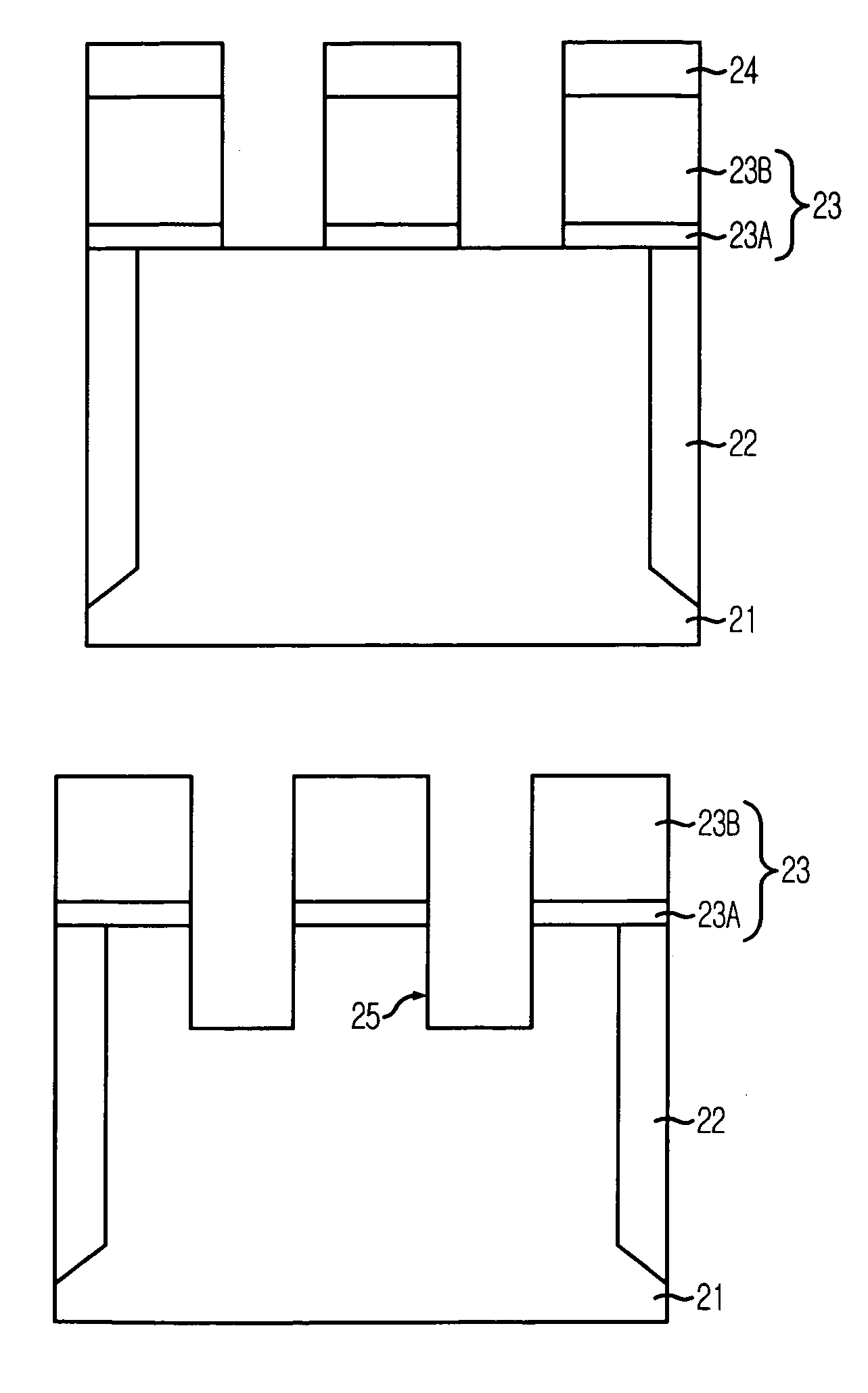
[0023] A method for fabricating a semiconductor device having a flask type recess gate consistent with embodiments of the present invention will be described in detail with reference to the accompanying drawings.

[0024]FIGS. 3A to 3G are cross-sectional views illustrating a method for fabricating a semiconductor device consistent with the present invention.

[0025] Referring to FIG. 3A, device isolation regions 22 are formed in a substrate 21 by employing a shallow trench isolation (STI) process. The device isolation regions 22 defining an active region are filled in trenches having a depth of approximately 3,000 Å or deeper using the STI process.

[0026] In more detail of the STI process, a pad oxide layer and a pad nitride layer are formed over the substrate 21, and masking and etching processes are performed to form the trenches. An insulation layer is filled into the trenches and a chemical mechanical polishing (CMP) process is performed to form the device isolation regions 22. Th...


PUM


Abstract

A method for fabricating a semiconductor device having a flask type recess gate includes forming a hard mask pattern on a substrate, etching the substrate to a predetermined depth using the hard mask pattern to form a first recess pattern, forming a passivation layer on sidewalls of the first recess pattern and the hard mask pattern, etching a bottom surface of the first recess pattern exposed by the passivation layer to form a second recess pattern, oxidizing sidewalls of the second recess pattern to form a silicon oxide layer, removing the passivation layer and the silicon oxide layer in sequential order, and forming a gate pattern over an intended recess pattern including the first recess pattern and the second recess pattern.

Description

RELATED APPLICATION [0001] The present application is based on and claims the benefit of priority to Korean patent application No. KR 2005-114949, filed in the Korean Patent Office on Nov. 29, 2005, the entire contents of which are incorporated herein by reference. [0002] 1. Technical Field [0003] The present invention relates to a method for fabricating a semiconductor device; and, more particularly, to a method for fabricating a semiconductor device having a flask type recess gate. [0004] 2. Description of Related Art [0005] As semiconductor devices become highly integrated, it is difficult to secure a refresh characteristic of a device during a typical forming process of a planar gate interconnection in which a gate is formed on a planarized active region. The difficulty is caused by a junction leakage generated from an increase of electric field as a gate channel length gradually decreases and a doping concentration of ion-implantation increases. [0006] A recess gate process is ...

Claims


Application Information

Patent Timeline
Patent Type & Authority Applications(United States)
IPC IPC(8): H01L21/3205H01L21/4763
CPCH01L29/4236H01L29/66621H01L21/18H10B99/00H10B12/00
Inventor HAN, KY-HYUNPARK, SANG-SOO
Owner SK HYNIX INC
Why Eureka
Try Eureka