Method of manufacturing semiconductor device having recess gate structure with varying recess width for increased channel length

a manufacturing method and technology of recess gate structure, applied in the direction of semiconductor devices, basic electric elements, electrical appliances, etc., can solve the problems of increasing electric field as well as function leakage of transistors, unable to meet the required threshold target of conventional transistors, and unable to keep up with technological demands. to achieve the effect of increasing the channel length

Active Publication Date: 2008-08-19
SK HYNIX INC
View PDF12 Cites 10 Cited by
  • Summary
  • Abstract
  • Description
  • Claims
  • Application Information

AI Technical Summary

Benefits of technology

[0009]Accordingly, the present invention has been made to solve the above-mentioned and other problems occurring in the prior art, and an object of the present invention is to provide a method of manufacturing a semiconductor device, which can sufficiently increase the channel length.
[0010]It is another object of the present invention to provide a method of manufacturing a semiconductor device, which can sufficiently increase the channel length, thereby effectively reducing current leakage and improving the refresh characteristics.
[0012]It is preferred that the first etching is performed by using a mixture solution in which HF, NH4F, HNO3, CH3COOH, H2O2 and H2O are mixed. The mixture solution may contain 1˜50% of CH3COOH solution. Also, the mixture solution may contain 1˜50% of HNO3 solution. It is also preferred that the first etching is performed at a temperature between 25 and 100° C. in order to improve an etching reactivity.

Problems solved by technology

The conventional transistors having planar structures are unable to keep up with the technological demands of the recent advances in the integration of DRAM devices, such that, for example, these conventional transistors are unable to meet the required threshold target of the device in which the transistors are integrated.
The advanced integration of DRAM devices requires reduction in the minimum feature size, and to reduce the minimum feature size the doping density is increased in a substrate, which inevitably increases the electric field as well as the function leakage in the transistor.
As a result, it is impossible to secure consistent reliability and yield for the devices with reduced active area.

Method used


Image

  • Method of manufacturing semiconductor device having recess gate structure with varying recess width for increased channel length
  • Method of manufacturing semiconductor device having recess gate structure with varying recess width for increased channel length
  • Method of manufacturing semiconductor device having recess gate structure with varying recess width for increased channel length

Examples


Embodiment Construction

[0023]Hereinafter, a preferred embodiment of the present invention will be described with reference to the accompanying drawings.

[0024]FIGS. 1A-1E are cross-sectional views for illustrating a method of manufacturing a semiconductor device according to an embodiment of the present invention.

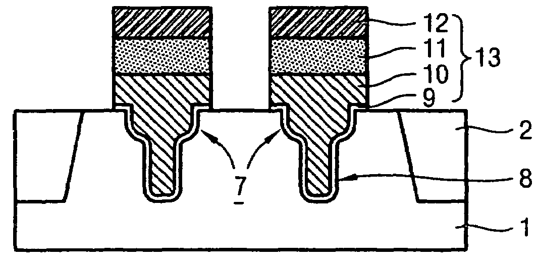
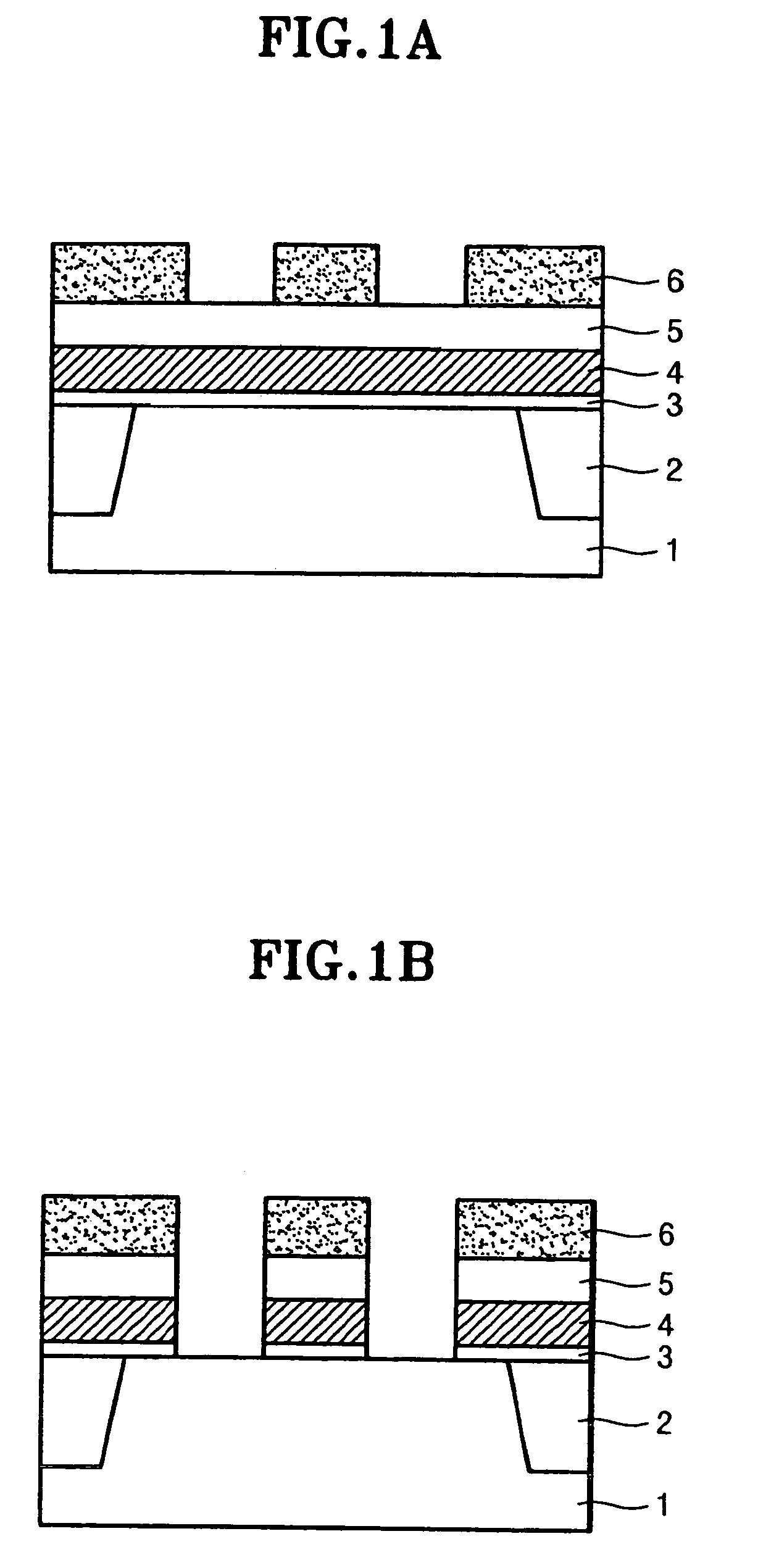
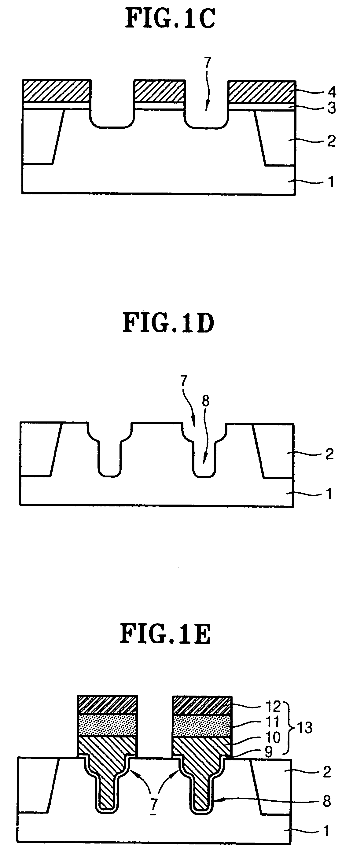
[0025]Referring to FIG. 1A, an active area defined by two portions of isolation layer 2 is formed in a semiconductor substrate 1. Then, an oxide layer 3 and a poly-silicon layer 4 are sequentially formed on the active area and the portions of the isolation layer 2 in the semiconductor substrate 1. Thereafter, a reflection-proof layer 5 is formed on the poly-silicon layer 4, and a mask pattern 6 is formed on the reflection-proof layer 5 to define the areas that are to be recessed (or etched) into the substrate 1.

[0026]In the present embodiment, a poly-silicon layer 4 is used as a hard mask for forming recesses in the substrate 1. However, it is possible to use an insulation layer such as a nitride ...


PUM


Abstract

A varying-width recess gate structure having a varying-width recess formed in a semiconductor device can sufficiently increase the channel length of the transistor having a gate formed in the varying-width recess, thereby effectively reducing the current leakage and improving the refresh characteristics. In the method of manufacturing the recess gate structure, etching is performed twice or more, so as to form a gate recess having varying width in the substrate, and a gate is formed in the gate recess.

Description

BACKGROUND OF THE INVENTION[0001]1. Field of the Invention[0002]The present invention relates generally to a method of manufacturing a semiconductor device, and more particularly to a method of manufacturing a semiconductor device having recess structure for increased channel length.[0003]2. Description of the Prior Art[0004]The conventional transistors having planar structures are unable to keep up with the technological demands of the recent advances in the integration of DRAM devices, such that, for example, these conventional transistors are unable to meet the required threshold target of the device in which the transistors are integrated. The advanced integration of DRAM devices requires reduction in the minimum feature size, and to reduce the minimum feature size the doping density is increased in a substrate, which inevitably increases the electric field as well as the function leakage in the transistor.[0005]Therefore, a three-dimensional active structure called a “recess ga...

Claims


Application Information

Patent Timeline
Patent Type & Authority Patents(United States)
IPC IPC(8): H01L21/3205
CPCH01L21/28061H01L21/30604H01L29/66621H01L21/3081H01L21/3065H01L21/18
Inventor KIM, JONG MANLEE, CHANG GOOKIM, JONG SIKWON, SE RA
Owner SK HYNIX INC
Why Eureka
Try Eureka