LDMOS ESD(Laterally Diffused Metal Oxide Semiconductor Electro-Static Discharge) structure

A source and drain technology, applied in electrical components, circuits, semiconductor devices, etc., can solve the problems of increasing IC design cost and device size, and achieve enhanced antistatic capability, increased effective channel length, and effective channel length. The effect of increasing the channel resistance

Active Publication Date: 2012-03-14
SEMICONDUCTOR MANUFACTURING INTERNATIONAL (BEIJING) CORP +1
View PDF5 Cites 12 Cited by
  • Summary
  • Abstract
  • Description
  • Claims
  • Application Information

AI Technical Summary

Problems solved by technology

[0017] The purpose of the present invention is to provide an LDMOS ESD structure to solve the problem that the existing LDMOS ESD increases the antistatic ability by increasing the channel length L, which causes the device size of the LDMOS ESD to increase, thereby increasing the IC design cost.

Method used


Image

  • LDMOS ESD(Laterally Diffused Metal Oxide Semiconductor Electro-Static Discharge) structure
  • LDMOS ESD(Laterally Diffused Metal Oxide Semiconductor Electro-Static Discharge) structure
  • LDMOS ESD(Laterally Diffused Metal Oxide Semiconductor Electro-Static Discharge) structure

Examples


Embodiment Construction

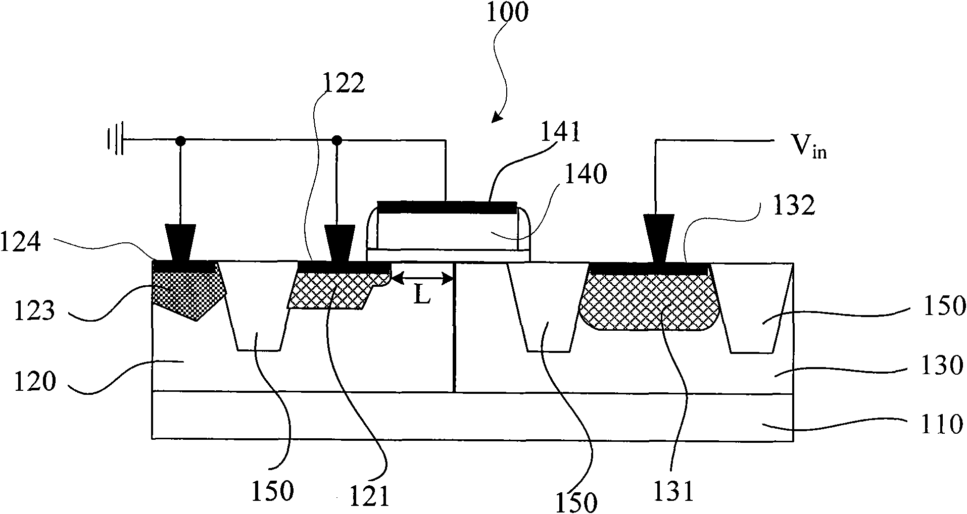
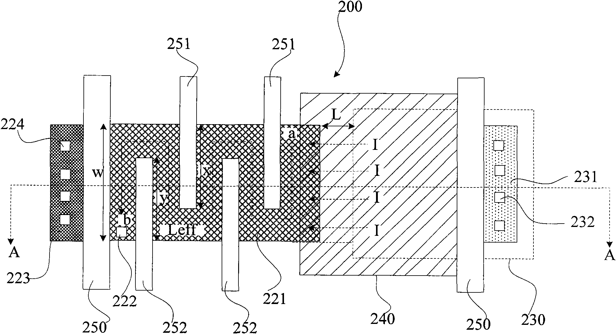
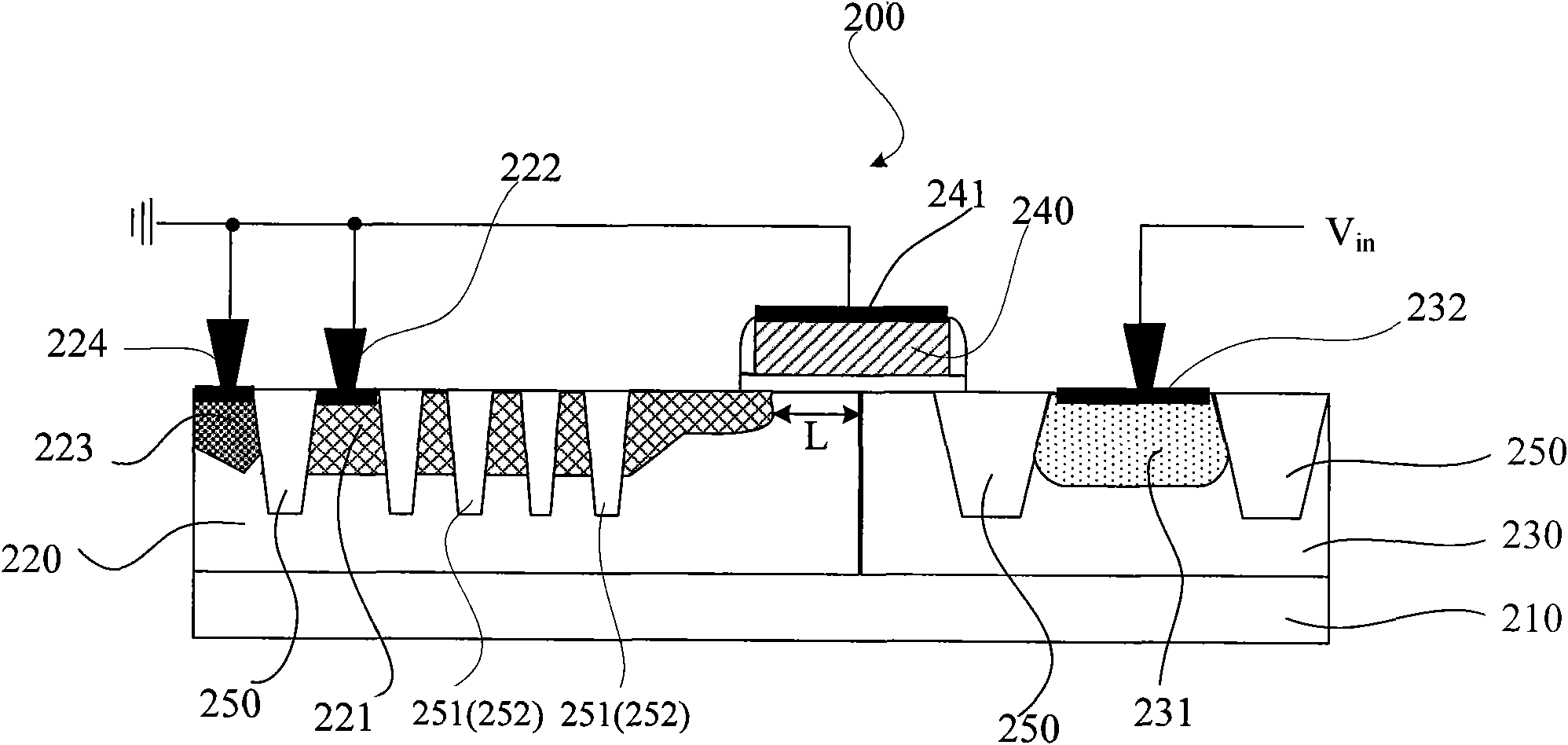
[0033] The LDMOS ESD structure proposed by the present invention will be further described in detail below in conjunction with the drawings and specific embodiments. Advantages and features of the present invention will be apparent from the following description and claims. It should be noted that the drawings are all in a very simplified form and use imprecise ratios, which are only used to facilitate and clearly assist the purpose of illustrating the embodiments of the present invention.

[0034] The core idea of ​​the present invention is to provide an LDMOS ESD structure, the LDMOS ESD structure is provided with an interdigitated STI structure in the source region, so that the flow direction of the electrostatic discharge current of the LDMOS ESD is in a square wave shape, thereby Without increasing the actual channel length, the effective channel length is increased, the effective channel resistance is increased, the holding voltage is further increased, and the antistati...


PUM


Abstract

The invention discloses an LDMOS ESD(Laterally Diffused Metal Oxide Semiconductor Electro-Static Discharge) structure comprising a gate region, a drain region and a source region, wherein an interdigitated STI(Shallow-Trench Isolation) structure is arranged in the source region, so that the flow direction of the electrostatic leakage current of the LDMOS ESD is of a square-wave form. Therefore, the effective channel length is increased while the actual channel length is not increased, and the effective channel resistance is increased, thereby further increasing the sustaining voltage and enhancing the antistatic effect of the LDMOS ESD.

Description

technical field [0001] The invention relates to the technical field of integrated circuits, in particular to an LDMOS ESD structure which can effectively reduce device size. Background technique [0002] As the level of integrated circuit manufacturing technology enters the deep submicron era of integrated circuit line width, the feature size of CMOS technology continues to shrink, and the ability of transistors to withstand high voltage and high current continues to decrease. Deep submicron CMOS integrated circuits are more susceptible to electrostatic shock failure, resulting in a decrease in product reliability. [0003] Static electricity is ubiquitous in the process of chip manufacturing, packaging, testing and use. The accumulated static charge is released in nanoseconds to microseconds with a current of several amperes or tens of amperes. The instantaneous power is as high as hundreds of kilowatts, and the discharge energy It can reach millijoules, and the destructio...

Claims


Application Information

Patent Timeline
Patent Type & Authority Applications(China)
IPC IPC(8): H01L29/78H01L29/08
CPCH01L29/7835H01L29/0653H01L29/0692
Inventor 曹国豪郑大燮陈德艳
Owner SEMICONDUCTOR MANUFACTURING INTERNATIONAL (BEIJING) CORP
Why Eureka
Try Eureka