Connecting structure and method for manufacturing the same

a technology of connecting structure and manufacturing method, applied in the direction of basic electric elements, electrical apparatus, semiconductor devices, etc., can solve the problems of retention time, impairment of low, increase of leakage current between storage capacitors b>3, etc., and achieve favorable topology of connection and extended channel length of resulting transistor

Inactive Publication Date: 2007-02-08
INFINEON TECH AG
View PDF8 Cites 9 Cited by
  • Summary
  • Abstract
  • Description
  • Claims
  • Application Information

AI Technical Summary

Benefits of technology

[0022] According to the invention, the electrically conducting material can be deposited substantially above the substrate surface. The expression “substantially above” means that there is more electrically conducting material above the substrate surface than below the substrate surface. In particular, the thickness of the conducting material above the substrate surface is larger than the thickness of the conducting material below the substrate surface. Preferably, in this case, the surface of the polysilicon filling which fills up the capacitor trench is at the same level as the substrate surface. The connection is thus provided above the substrate surface and extends in the connecting area which is adjacent to the substrate surface to somewhat below the substrate surface. More specifically, the electrically conducting material extends 30 to 40 nm above the substrate surface and 0 to 10 nm below the substrate surface. In this case, the advantage is that the connecting structure provides a contact to the substrate surface. Accordingly, the length of the channel of a resulting transistor will be extended.
[0023] Alternatively, the electrically conducting material can be deposited substantially below the substrate surface. In this connection, “substantially below” means that more electrically conducting material is provided below the substrate surface than above the substrate surface. In particular, this expression means that the electrically conducting material extends up to 10 nm maximum above the substrate surface. To put it more precisely, the electrically conducting material extends 0 to 10 nm above the substrate surface and 30 to 40 nm below the substrate surface. In this case, the special advantage will result that a connecting structure is provided through which the longest possible channel of a resulting transistor will be ensured and that, nonetheless, a more favorable topology of the connection is achieved.

Problems solved by technology

However, shortening this channel length results in an increase of leakage currents between storage capacitor 3 and bit line 52.
Overall, a reduced channel length can result in an impairment of the low threshold leakage current and thus the retention time, i.e., the time within which information can again be recognizably stored in the memory cell.

Method used


Image

  • Connecting structure and method for manufacturing the same
  • Connecting structure and method for manufacturing the same
  • Connecting structure and method for manufacturing the same

Examples


Embodiment Construction

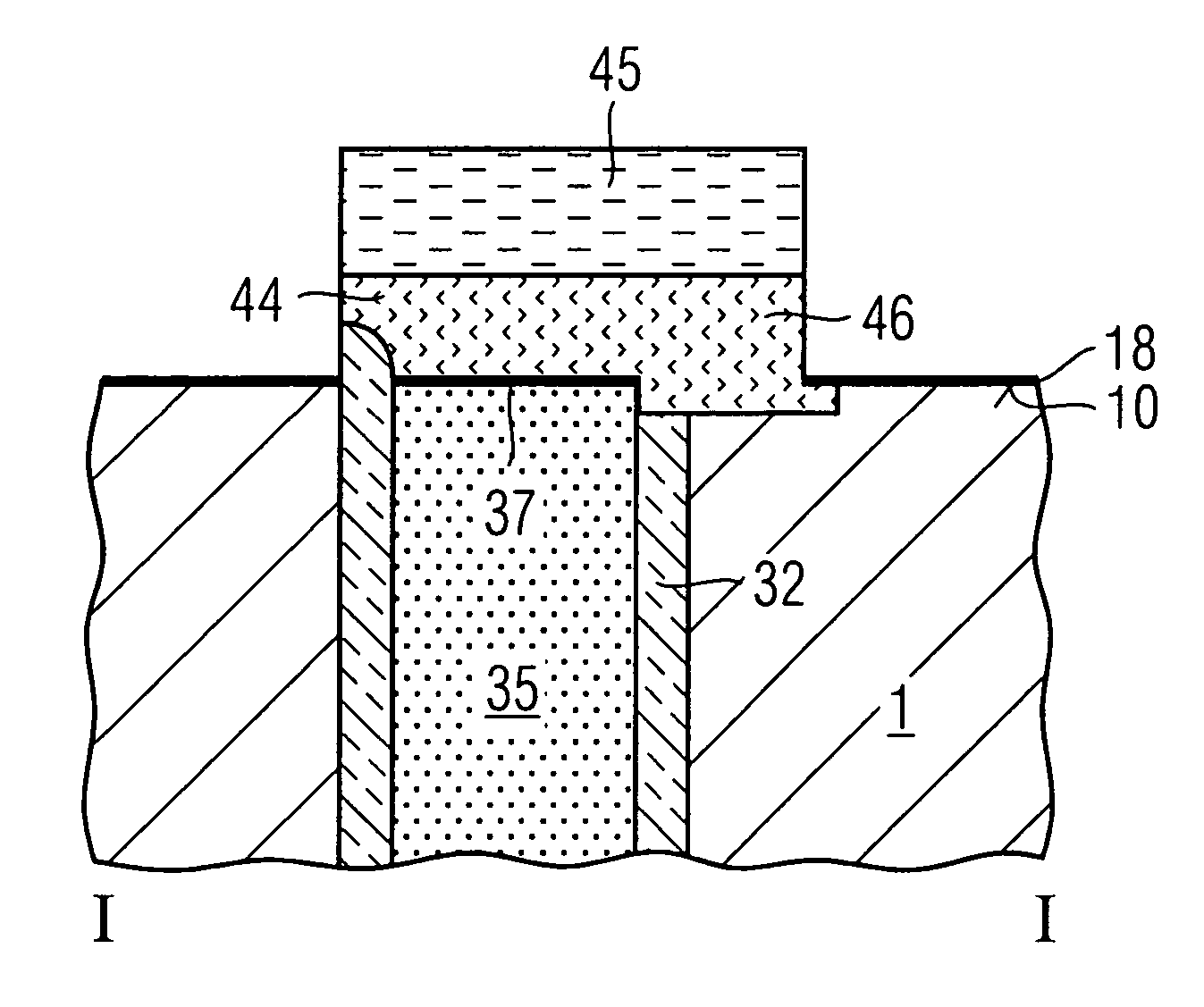
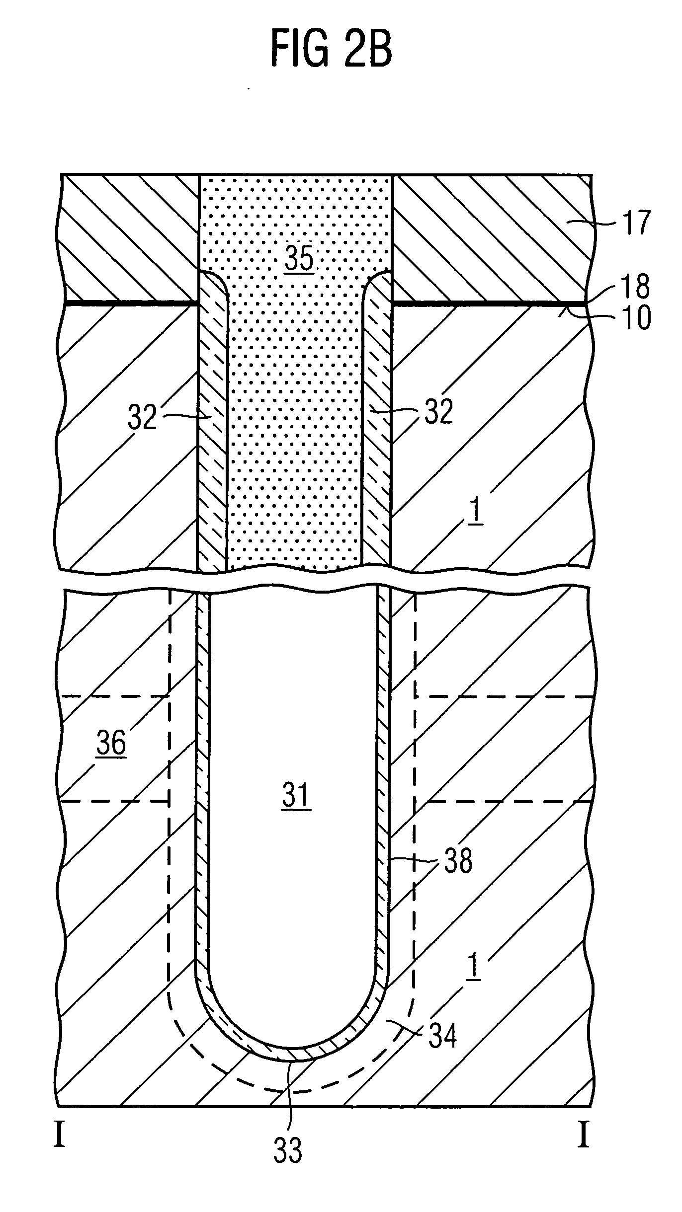
[0033]FIGS. 2A and 2B respectively present a top plan view and a cross-sectional side view in elevation of a storage capacitor which is provided in a trench 38 formed in a semiconductor substrate 1, for example, a silicon substrate. The trench normally has a depth of 6 to 7 μm and can be designed as illustrated in FIG. 2B in cross section, or it can be widened in its lower portion.

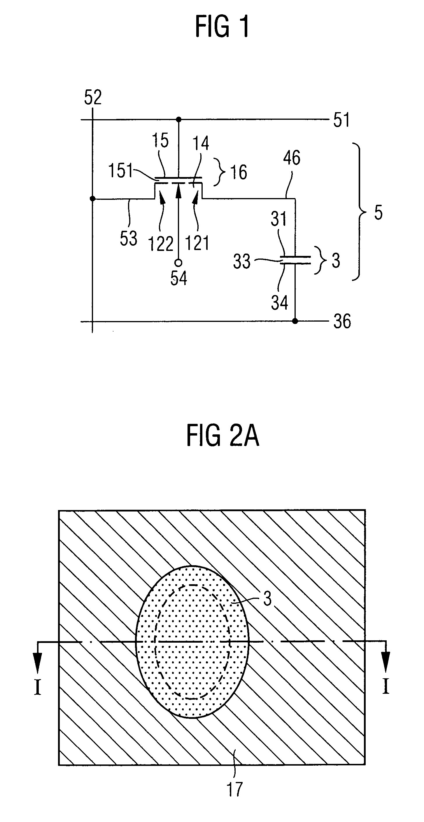
[0034] As illustrated in FIG. 2A, the larger diameter of the capacitor trench is typically 2 F while the smaller diameter is 1.5 F. F is the minimum structural size and can currently be 90 to 110 nm and especially less than 90 nm. FIG. 2B is a cross-sectional view along line I-I as illustrated in FIG. 2A. The counter-electrode 34 of the storage capacitor is realized, for example, by an n+ doped substrate portion. In the trench 38 are arranged, moreover, a capacitor dielectric 33 as normally used, as well as a polysilicon filling 31 as a storage electrode. The upper trench portion provides an isolation col...


PUM


Abstract

A method for manufacturing a surface strap connection between a trench capacitor and a selection transistor includes providing a masking material on a surface of a semiconductor substrate in areas where no trench capacitors have been formed. An undoped semiconductor layer having vertical and horizontal areas is applied. An oblique ion implantation is performed such that a vertical area of the semiconductor layer on which the connecting structure is to be formed is not doped. After removal of the undoped portion of the semiconductor layer, the exposed portion of the masking material is laterally etched, one part of the substrate surface is exposed, and the doped part of the semiconductor layer is removed. An electrically conducting connection material is applied so that an electrical contact exists between the exposed portion of the substrate surface and the storage electrode.

Description

CROSS REFERENCE TO RELATED APPLICATIONS [0001] This application claims priority under 35 U.S.C. §119 to German Application No. DE 10 2005 036 561.2, filed on Aug. 3, 2005, and titled “Connecting Structure and Method for Manufacturing a Connecting Structure,” the entire contents of which are hereby incorporated by reference. FIELD OF THE INVENTION [0002] This invention relates to a method for manufacturing a connecting structure between a trench capacitor and an access transistor as well as to a corresponding connecting structure. BACKGROUND [0003] Memory cells of dynamic random access memories (DRAMs) generally comprise a storage capacitor and an access transistor. The storage capacitor stores information in the form of an electrical charge representing a logical value 0 or 1. By controlling the readout or, respectively, the access transistor via a word line, the information stored in the storage capacitor can be read out via a bit line. For secure storage of the charge and to permi...

Claims


Application Information

Patent Timeline
Patent Type & Authority Applications(United States)
IPC IPC(8): H01L21/20
CPCH01L27/10867H10B12/0385
Inventor HEINECK, LARSPOPP, MARTIN
Owner INFINEON TECH AG
Why Eureka
Try Eureka