Solid-state imaging apparatus

A camera device, solid-state technology, applied in the direction of image communication, TV, color TV components, etc., can solve the problems of readout output signal influence, noise, technical difficulties, etc., and achieve the effect of preventing image quality from deteriorating

Inactive Publication Date: 2009-08-12
OLYMPUS CORP
View PDF7 Cites 0 Cited by
  • Summary
  • Abstract
  • Description
  • Claims
  • Application Information

AI Technical Summary

Problems solved by technology

[0007] However, in a solid-state imaging device having a pixel unit composed of pixels with the above-mentioned structure, in order to adopt the integral shutter method, the photoelectric conversion units of all pixels collectively perform discharge reset operations based on the discharge control signal φTX2 during the readout period. Depends on the number of pixels and pixel size, but it needs to drive a load capacitance of tens of thousands of pF as a whole
When performing such a drive, such as Figure 16 As shown, the power supply (Vdd) and Gnd fluctuate, which affects the readout output signal (readout), produces banded noise, and degrades the image quality.
In addition, it is technically very difficult to complete such an exhaust reset operation that is driven as a whole during the horizontal blanking period (several μs or less).

Method used


Image

  • Solid-state imaging apparatus
  • Solid-state imaging apparatus
  • Solid-state imaging apparatus

Examples


Embodiment 1

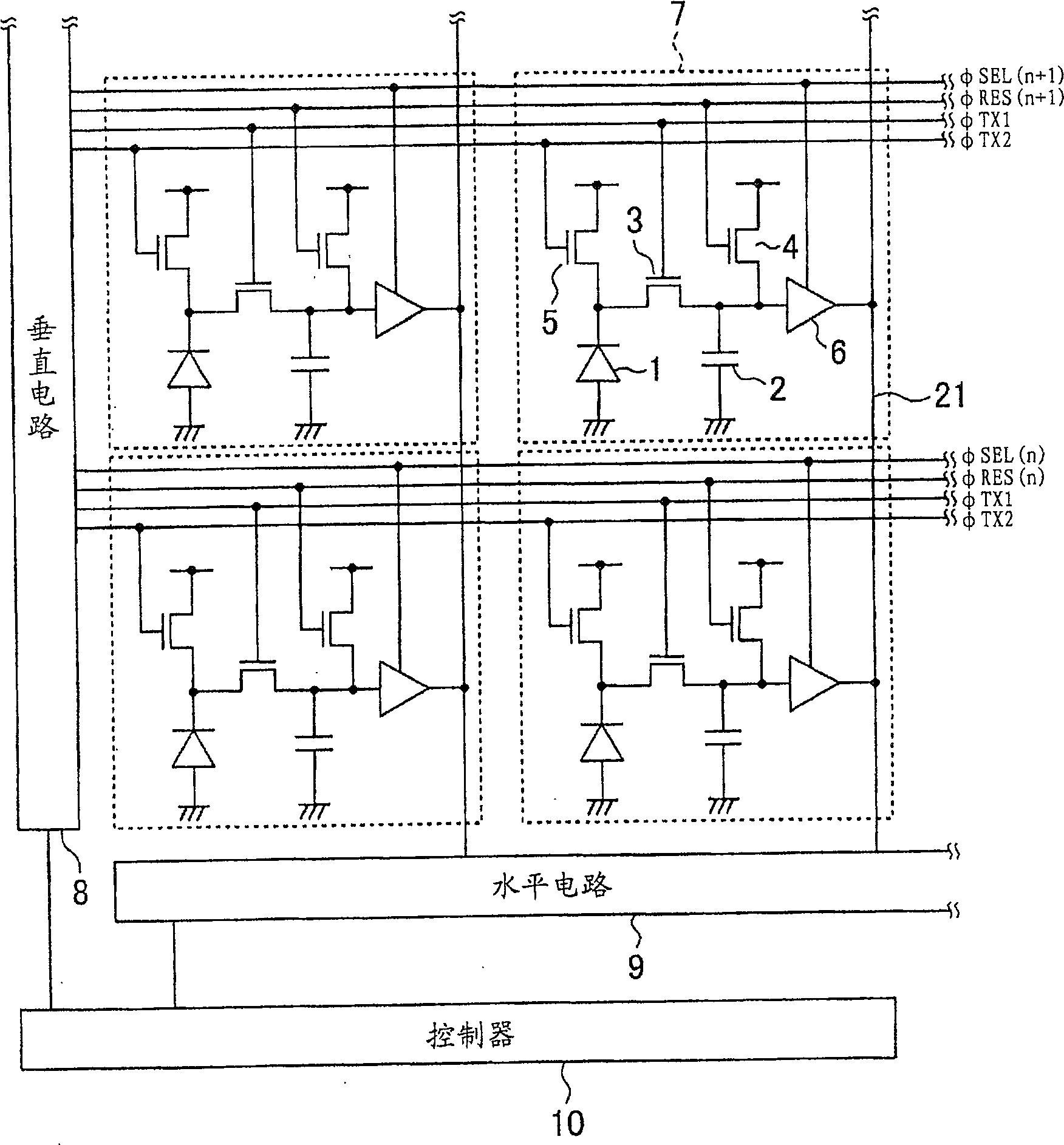
[0038] First, Embodiment 1 of the solid-state imaging device according to the present invention will be described. figure 1 It is a schematic circuit block diagram of the solid-state imaging device according to the first embodiment. exist figure 1 Among them, 1 is a photoelectric conversion unit such as a photodiode, which is used to receive light for a predetermined time, accumulate photoelectric charges, and perform photoelectric conversion; 2 is a storage unit for holding photoelectric charges in the photoelectric conversion unit 1; 3 is a photoelectric conversion unit 1 4 is a reset unit (corresponding to the first reset unit of the claim) that resets the storage unit 2 to the power supply potential; 5 is a discharge that resets the photoelectric conversion unit 1 to the power supply potential Unit (corresponding to the second reset unit of the claim); 6 is a readout unit for reading out the charge of the memory unit 2, and 7 is a unit pixel composed of the above-mentio...

Embodiment 2

[0047] Next, use Figure 5 Embodiment 2 of the solid-state imaging device according to the present invention will be described. The difference in configuration between the solid-state imaging device according to the second embodiment and the solid-state imaging device according to the first embodiment lies in that an additional function for performing A processing on the signal read out from the readout unit 6 of each pixel via the horizontal circuit 9 is added. A / D converter 11 for A / D conversion, line memory 12 for delaying the signal after A / D conversion by A / D converter 11, and line memory 12 for selecting from A / D converter 11 and line memory 12, the controller 10 controls the operation of these line memories 12 and the selection unit 13. In addition, other structural parts are the same as in the first embodiment.

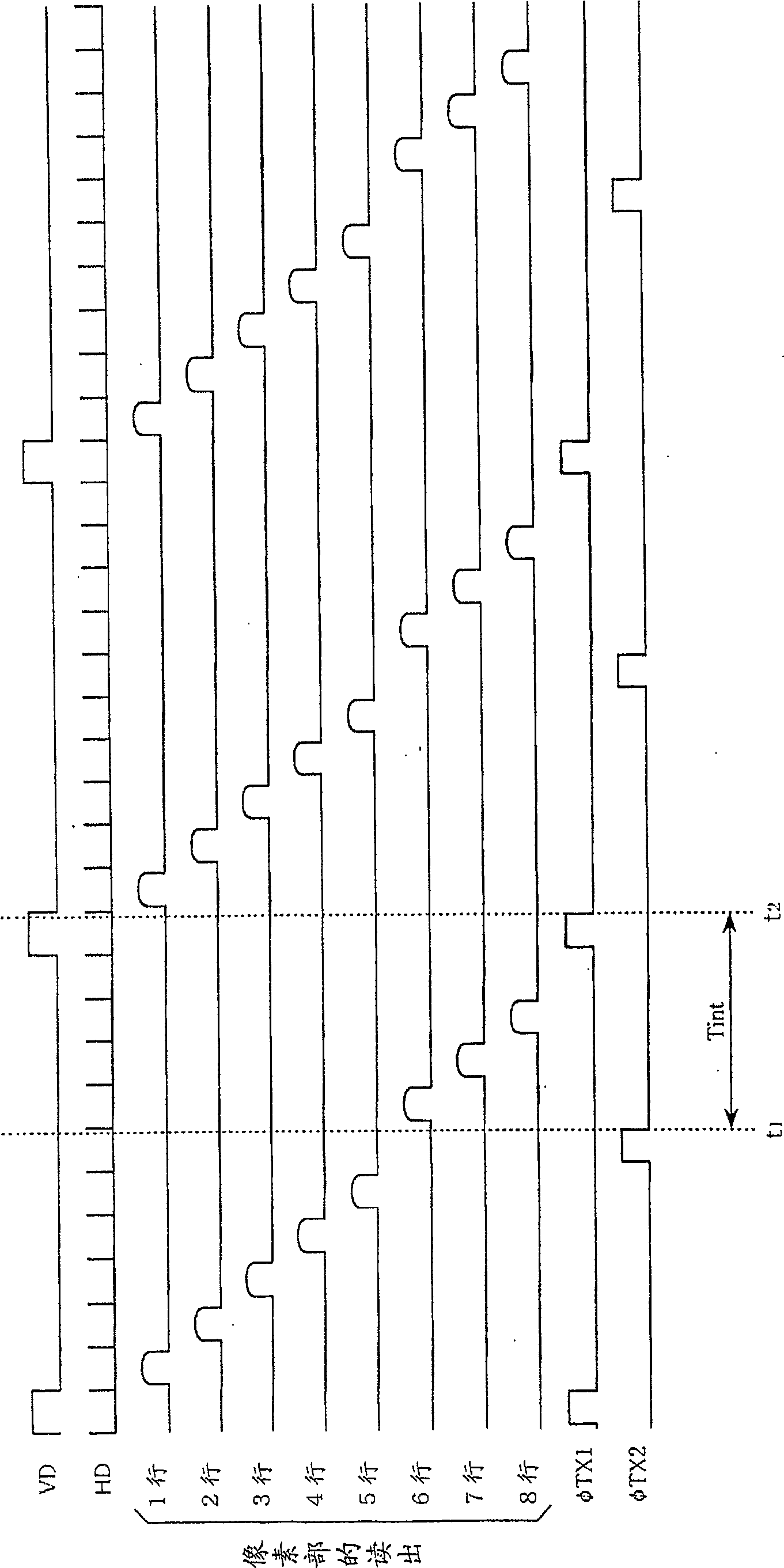
[0048] Next, refer to Figure 6 The shown timing charts explain the operation of the solid-state imaging device according to the second embodiment. exist ...

Embodiment 3

[0055] Next, use Figure 9Embodiment 3 of the solid-state imaging device according to the present invention will be described. The difference in configuration between the solid-state imaging device according to the third embodiment and the solid-state imaging device according to the first embodiment lies in the addition of an A A / D converter 11 for / D conversion, a buffer memory 15 for temporarily storing a signal A / D converted by the A / D converter 11, and a memory controller 14 for controlling the buffer memory 15, controlled by The memory controller 10 controls the operation of the memory controller 14. In addition, other structural parts are the same as in the first embodiment.

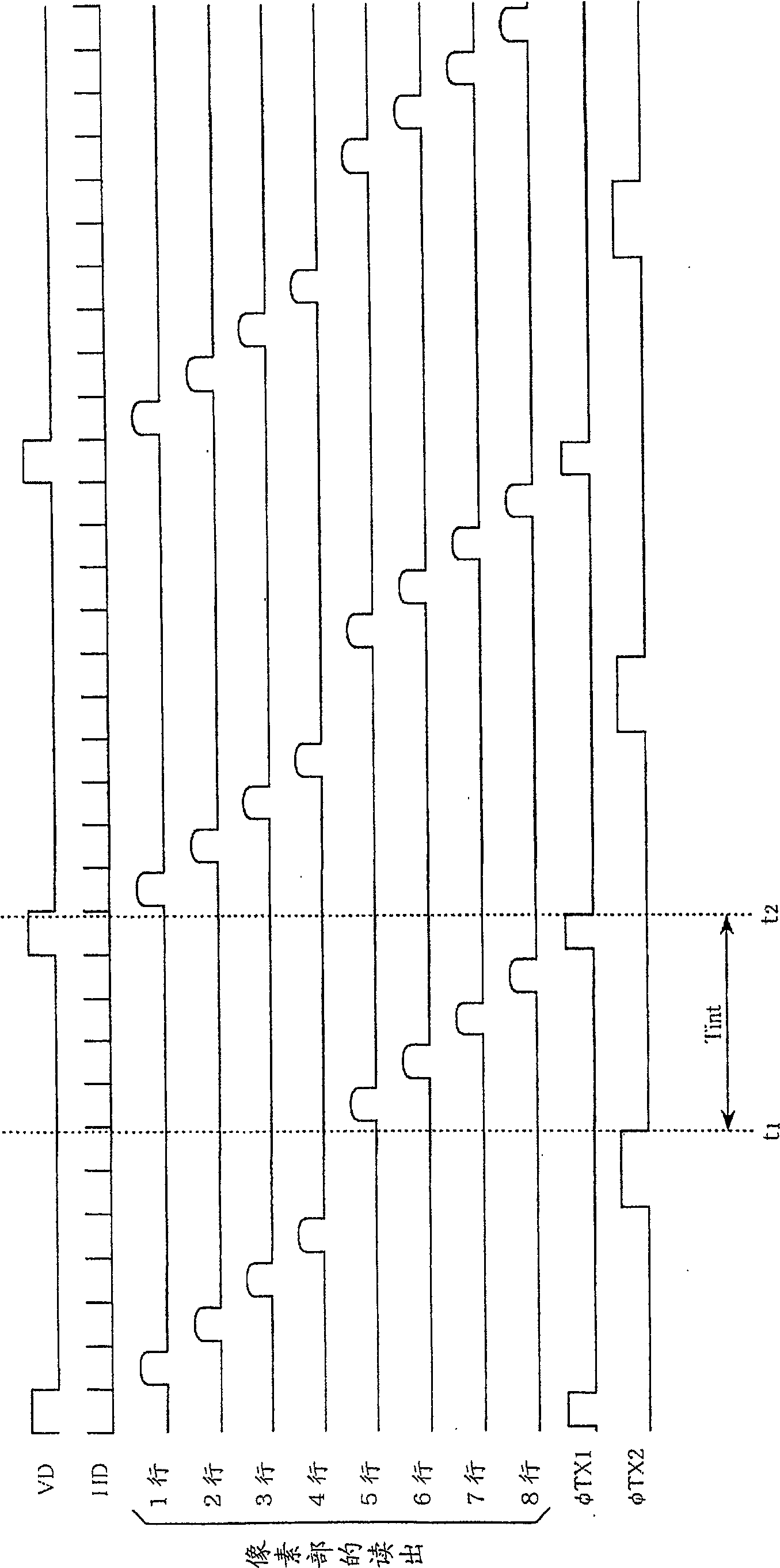
[0056] Next, refer to Figure 10 The shown timing charts explain the operation of the solid-state imaging device according to the third embodiment. exist Figure 10 Among them, the blocks represented as S1, S2, S3, ..., S8 in the output column of the A / D converter 11 are read out from the read...


PUM


Abstract

The invention provides a solid imaging device to prevent an influence brought by the change of a GND or a power supply having a whole shutter function caused by pixels whole resetting. Following controls are carried out by a controller (10): after the photoelectric switching units (1) of all pixels in a readout target area are reset wholly with a discharging unit (5) and after a predetermined period, a photoelectric switching signal is transmitted wholly by a transmitting unit (3) from all the pixel photoelectric switching units to a memorizing unit (2), when the signal memorized in the memorizing unit is read by a reading unit (6), if the discharging unit is reset wholly during the reading unit working, the reading carried out by the reading unit is paused temporally.

Description

technical field [0001] The present invention relates to a solid-state imaging device, and more particularly, to a solid-state imaging device capable of avoiding the influence of fluctuations in power supply and GND due to a reset operation of all pixels in a readout area. Background technique [0002] Conventionally, as a pixel used in a pixel portion of a solid-state imaging device having a global shutter (also referred to as a global shutter) function, for example, Japanese Patent Application Laid-Open No. 11-261896 discloses Figure 15 Pixels of the structure shown. exist Figure 15 Among them, 1 is a photoelectric conversion unit such as a photodiode, which is used to receive light for a predetermined time, accumulate photoelectric charges, and perform photoelectric conversion; 2 is a storage unit for holding photoelectric charges in the photoelectric conversion unit 1; 3 is a photoelectric conversion unit 1 4 is a reset unit that resets the storage unit 2 to a power sup...

Claims


Application Information

Patent Timeline
Patent Type & Authority Patents(China)
IPC IPC(8): H04N5/335H04N3/15H04N5/353H04N5/357H04N5/363H04N5/374H04N5/376
CPCH04N5/3658H04N5/3456H04N5/3532H04N5/3577H04N25/445H04N25/531H04N25/617H04N25/677
Inventor 中岛慎一
Owner OLYMPUS CORP
Why Eureka
Try Eureka