Power semiconductor characteristic parameter test system

A technology for power semiconductors and characteristic parameters, which is applied in the direction of single semiconductor device testing, electrical measurement, and measurement devices, which can solve the problems of time-consuming and high cost.

Pending Publication Date: 2021-06-18
ELECTRIC POWER RES INST OF STATE GRID ZHEJIANG ELECTRIC POWER COMAPNY +2
View PDF4 Cites 0 Cited by
  • Summary
  • Abstract
  • Description
  • Claims
  • Application Information

AI Technical Summary

Problems solved by technology

[0007] The technical problem to be solved by the present invention is to overcome the defect that the above-mentioned existing test equipment needs to be rebuilt when testing different items, which is not only time-consuming and costly, but also to provide a power semiconductor with complete testing functions and flexible adjustment according to the test items. Parametric test system, by quickly switching to the matching test circuit, it takes less time and costs less

Method used


Image

  • Power semiconductor characteristic parameter test system
  • Power semiconductor characteristic parameter test system
  • Power semiconductor characteristic parameter test system

Examples


Embodiment Construction

[0032] The present invention will be described in further detail below in conjunction with the accompanying drawings.

[0033] This embodiment is only an explanation of the present invention, and it is not a limitation of the present invention. Those skilled in the art can make modifications to this embodiment without creative contribution as required after reading this specification, but as long as the claims of the present invention are protected by patent law.

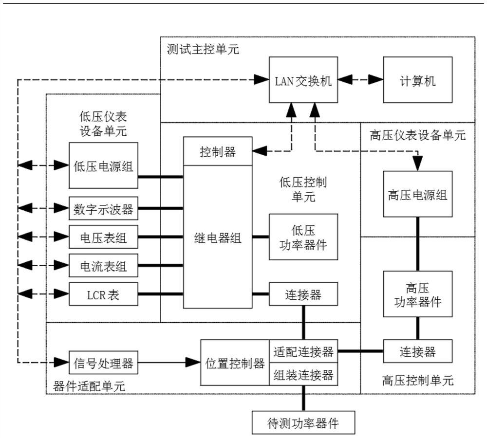
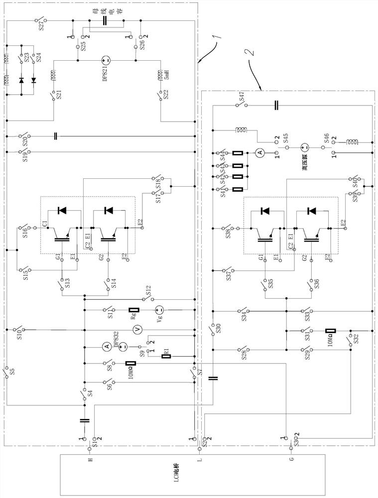
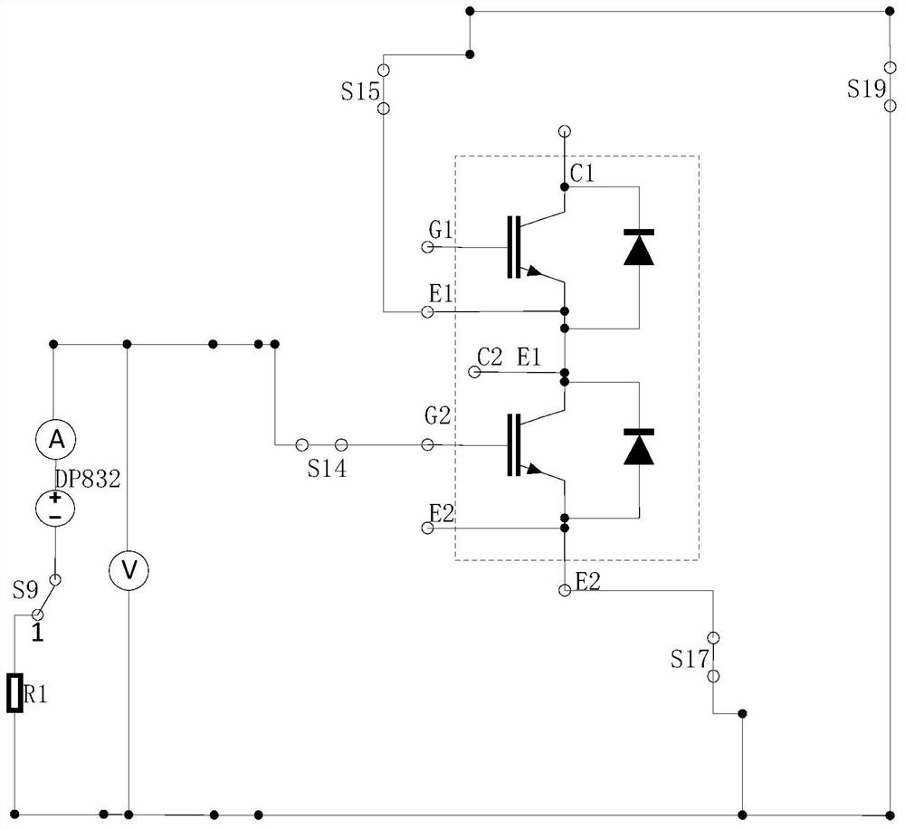
[0034] Such as figure 1 As shown, the present invention provides a power semiconductor characteristic parameter test system. By integrating the test circuits of various characteristic parameters, the test circuits of each characteristic parameter are integrated into a test system. When using it, according to the current test items The test circuit is switched through the relay group to complete the test of multiple characteristic parameters of the power semiconductor devices IGBT, MOSFET and diode.

[0035] The te...


PUM


Abstract

The invention relates to the technical field of power semiconductor characteristic parameter testing, and provides a power semiconductor characteristic parameter testing system which comprises a low-voltage instrument equipment unit, a low-voltage control unit, a high-voltage instrument equipment unit, a high-voltage control unit, a device adaptation unit and a testing main control unit. The low-voltage control unit comprises a low-voltage project related component and a relay group; the relay groups are respectively arranged among the low-voltage item related parts, the low-voltage instrument equipment unit and the power device to be tested and preset corresponding conduction states according to different types of low-voltage parameter test items; the relay group enables the low-voltage item related component, the low-voltage instrument equipment unit and the to-be-tested power device to switch the connection state according to a preset conduction state so as to form a test circuit corresponding to the test item; and test circuits of low-voltage test items are integrated together, the test connection mode can be changed through the relay set, and switching of different test items is automatically achieved.

Description

technical field [0001] The invention relates to the technical field of power semiconductor characteristic parameter testing, in particular to a power semiconductor characteristic parameter testing system. Background technique [0002] Among all power semiconductor devices, fully controlled devices represented by MOSFET (Metal-Oxide-Semiconductor Field-Effect Transistor) and IGBT (Insulated Gate Bipolar Transistor) are represented by Its excellent comprehensive characteristics such as voltage drive, low loss, and fast switching have won large-scale applications in many fields. [0003] In order to ensure the effective use of power semiconductor devices in power electronic systems, it is necessary to test the characteristic parameters of the devices before use. With the development of higher voltage and larger capacity devices and modules, it is necessary to test their characteristic parameters. The test system also puts forward new requirements. [0004] In order to fully u...

Claims


Application Information

Patent Timeline
Patent Type & Authority Applications(China)
IPC IPC(8): G01R31/26
CPCG01R31/2601
Inventor 王异凡龚金龙杨青刘黎王一帆孙明林氦邓志江曾振源张斌陈少华宋琦华周迅张显堡黄继来
Owner ELECTRIC POWER RES INST OF STATE GRID ZHEJIANG ELECTRIC POWER COMAPNY
Why Eureka
Try Eureka