Supercharge Your Innovation With Domain-Expert AI Agents!

Active pixel image sensor and display device

An image sensor and pixel technology, applied in the direction of radiation control devices, transistors, diodes, etc., can solve the problems of affecting the sensing ability of the sensor, high off-state current, poor stability, etc.

Pending Publication Date: 2021-06-22
BOE TECH GRP CO LTD
View PDF0 Cites 2 Cited by
  • Summary
  • Abstract
  • Description
  • Claims
  • Application Information

AI Technical Summary

Problems solved by technology

[0004] However, the thin-film transistors in the combination technology of the existing source image sensor and the PIN junction adopt low-temperature polysilicon (LTPS) technology, and the main problems of the LTPS technology are poor stability and high off-state current, which affect the sensing of the sensor. ability

Method used


Image

  • Active pixel image sensor and display device
  • Active pixel image sensor and display device
  • Active pixel image sensor and display device

Examples


Embodiment Construction

[0043] The technical solutions in the embodiments of the present invention will be clearly and completely described below with reference to the accompanying drawings in the embodiments of the present invention. Obviously, the described embodiments are only a part of the embodiments of the present invention, but not all of the embodiments. Based on the embodiments of the present invention, all other embodiments obtained by those of ordinary skill in the art without creative efforts shall fall within the protection scope of the present invention.

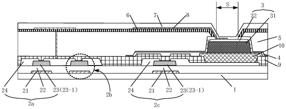
[0044] Please refer to figure 1 With the shown structure, the embodiment of the present application provides an active pixel image sensor, including: a substrate 1, a driving thin film transistor 2a, a reset thin film transistor 2b, a switching thin film transistor 2c, and a PIN functional layer 3, wherein the driving thin film transistor 2a, the reset thin film transistor 2b and the switching thin film transistor 2c are all formed on...


PUM


Abstract

The invention relates to the technical field of display, and discloses an active pixel image sensor and a display device. The active pixel image sensor comprises a substrate, a PIN functional layer, a driving thin film transistor, a reset thin film transistor and a switching thin film transistor, wherein each thin film transistor comprises a grid electrode, a grid insulating layer and an active layer which are stacked; the active layer in the driving thin film transistor at least comprises a first sub-active layer, and the preparation material of the first sub-active layer is an oxide material; the carrier concentration range of the preparation material of the first sub-active layer is 1*10E20-1*10E21, and the carrier Hall mobility range is 25-50cm <2> / Vs; and the active layer in the reset thin film transistor is prepared from an oxide material. According to the active pixel image sensor, the stability and mobility of a device can be improved, and an off-state current can be reduced.

Description

technical field [0001] The present invention relates to the field of display technology, in particular to an active pixel image sensor and a display device. Background technique [0002] In current display devices, passive image photosensitive sensors are generally used as photosensitive devices. However, the passive image photosensitive sensor has a low signal-to-noise ratio, and the sensor uses a driving chip to collect current to form image recognition. The image formed by this method has poor quality and low resolution, which cannot meet the needs of high-end products. [0003] In view of the above problems, a technology combining active image sensor and PIN junction is proposed. The advantage of this scheme is that the signal-to-noise ratio is high. The signal-to-noise ratio of the active image sensor is 5 times that of the passive image photosensitive sensor. The driver chip in the image sensor collects voltage signals, which may improve product performance. [0004]...

Claims


Application Information

Patent Timeline
IPC IPC(8): H01L27/146
CPCH01L27/14616H01L27/14643
Inventor 贺家煜宁策李正亮胡合合姚念琦赵坤黄杰雷利平刘雪
Owner BOE TECH GRP CO LTD
Features
  • R&D
  • Intellectual Property
  • Life Sciences
  • Materials
  • Tech Scout
  • Unparalleled Data Quality
  • Higher Quality Content
  • 60% Fewer Hallucinations
Learn More