
GIP circuit and driving method thereof

A technology of GIP circuit and driving method, which is applied in the direction of instruments, static indicators, etc., can solve problems such as the influence of gate circuit output waveform transistor leakage, and achieve the effect of solving the problem of abnormal screen display and stable output waveform

Pending Publication Date: 2021-06-29
FUJIAN HUAJIACAI CO LTD
View PDF6 Cites 0 Cited by
  • Summary
  • Abstract
  • Description
  • Claims
  • Application Information

AI Technical Summary

Problems solved by technology

[0004] Therefore, it is necessary to provide a GIP circuit and its driving method to solve the problem that the output waveform of the gate circuit is easily affected by the leakage of the transistor

Method used


Image

  • GIP circuit and driving method thereof
  • GIP circuit and driving method thereof

Examples


Embodiment Construction

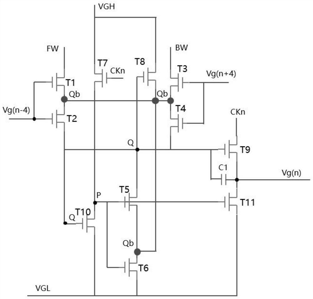
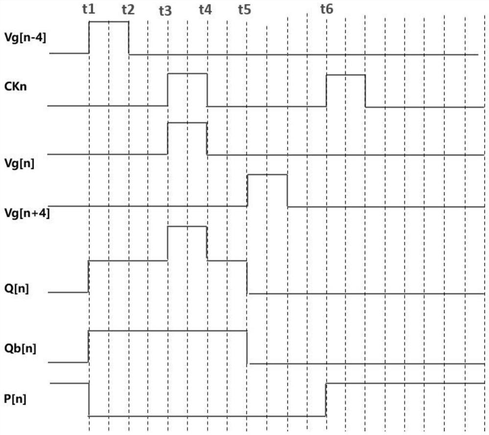
[0032] In order to explain in detail the technical content, structural features, achieved goals and effects of the technical solution, the following will be described in detail in conjunction with specific embodiments and accompanying drawings.

[0033] see Figure 1 to Figure 2 , the present application discloses a GIP circuit and its driving method, including: transistor T1, transistor T2, transistor T3, transistor T4, transistor T5, transistor T6, transistor T7, transistor T8, transistor T9, transistor T10, transistor T11 and Capacitor C1; the input terminal of the transistor T1 is connected to the voltage signal FW, the output terminal of the transistor T1 is connected to the Qb node, and the control terminal of the transistor T1 is connected to the gate G(n-4); the input terminal of the transistor T2 connected to the Qb node, the output terminal of the transistor T2 is connected to the Q node, the control terminal of the transistor T2 is connected to the gate G(n-4); the ...


PUM


Abstract

The invention discloses a GIP circuit and a driving method thereof. A T1 control end is connected with G(n-4); the input end of the T2 is connected with the Qb, the output end of the T2 is connected with the Q, the control end of the T2 is connected with the G(n-4), the output end of the T3 is connected with the Qb, and the control end of the T3 is connected with the G(n + 4); the input end of T4 is connected with Qb, the output end of T4 is connected with Q, and the control end of T4 is connected with G(n + 4); the input end of T5 is connected with Q, the output end of T5 is connected with Qb, and the control end of T5 is connected with P; the input end of the T6 is connected with the Qb, the control end of the T6 is connected with the P, the output end of the T7 is connected with the P, the output end of the T8 is connected with the Qb, and the control end of the T8 is connected with the Q; the output end of T9 is connected with G(n), and the control end of T9 is connected with Q; the input end of the T10 is connected with the P, and the control end of the T10 is connected with the Q; the input end of T11 is connected with G(n), and the control end of T11 is connected with P; one polar plate of C1 is connected with Q, and the other polar plate of C1 is connected with G(n). According to the technical scheme, the problem of picture display abnormity caused by output waveform abnormity is solved.

Description

technical field [0001] The invention relates to the field of display technology, in particular to a GIP circuit and a driving method thereof. Background technique [0002] For the display panel, the display quality of the picture is very important, and the display quality is closely related to the output waveform of the GIP circuit. When the output waveform of the GIP circuit is abnormal, it often causes display problems on the panel. [0003] In order to reduce the manufacturing cost of the display panel and achieve narrow frame, GIP (Gate in Panel) technology is usually used in the manufacturing process to directly integrate the gate circuit (ie, the GIP circuit) on the flat display panel. The output waveform of the GIP circuit is easily affected by the leakage of the transistor, which leads to distortion of the output waveform of the GIP circuit. The distorted output waveform will cause problems in turning on and off the transistors in the display area of ​​the display ...

Claims


Application Information

Patent Timeline
IPC IPC(8): G09G3/20G09G3/36
CPCG09G3/20G09G3/3696
Inventor 谢建峰
Owner FUJIAN HUAJIACAI CO LTD
Learn More