

Cleaning device for improving silicon wafer surface cleaning capacity and control method thereof
A silicon wafer surface and control method technology, applied in cleaning methods and utensils, cleaning methods using liquids, chemical instruments and methods, etc., can solve problems such as scratches on the surface of silicon wafers, achieve high operating stability, and solve mechanical A wound, the effect that the structure is simple
- Summary
- Abstract
- Description
- Claims
- Application Information
AI Technical Summary
Problems solved by technology
Method used
Image

Examples
Embodiment
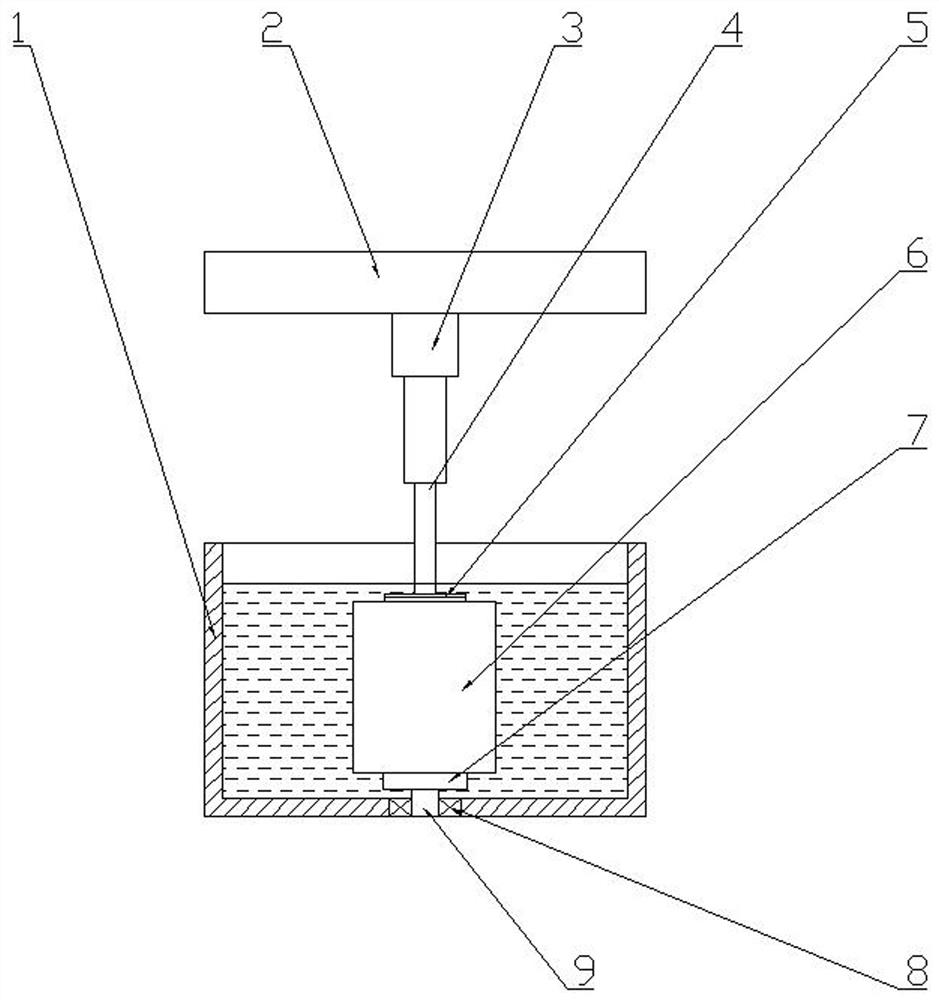
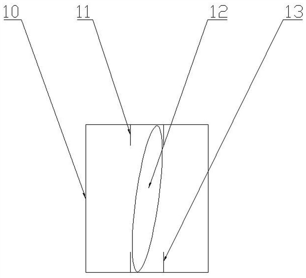
[0026] Example: such as figure 1 and figure 2 As shown, a cleaning device for improving the cleaning ability of the surface of a silicon wafer includes a cleaning tank 1, an upper frame 2 is arranged above the cleaning tank 1, a cleaning component 6 is arranged in the cleaning tank 1, and the lower end of the cleaning component 6 is connected to the cleaning tank 1. There is a rotating shaft 9 which is movable and nestedly connected with the cleaning tank 1, and a bearing 8 is arranged between the rotating shaft 9 and the cleaning tank 1. A tray 7 is provided between the rotating shaft 9 and the cleaning assembly 6 . A lift cylinder 4 is provided between the cleaning assembly 6 and the upper frame 2, and a connecting flange 5 is provided between the lift cylinder 4 and the cleaning assembly 6. A rotary motor 3 is arranged between the lifting cylinder 4 and the upper frame 2 . Cleaning assembly 6 comprises sheet box 10, and sheet box 10 is provided with 10 silicon wafers 12...
PUM
 Abstract
Description
Claims
Application Information