

Biasing circuit for radio frequency power amplifier
A technology of radio frequency power and bias circuit, which is applied to high-frequency amplifiers and improved amplifiers to reduce temperature/power supply voltage changes. It can solve problems such as gain collapse, poor temperature compensation effect, and emitter voltage drop, so as to improve temperature compensation. effect of effect
Active Publication Date: 2021-07-13
GUANGDONG UNIV OF TECH
View PDF5 Cites 5 Cited by
- Summary
- Abstract
- Description
- Claims
- Application Information
AI Technical Summary
Problems solved by technology
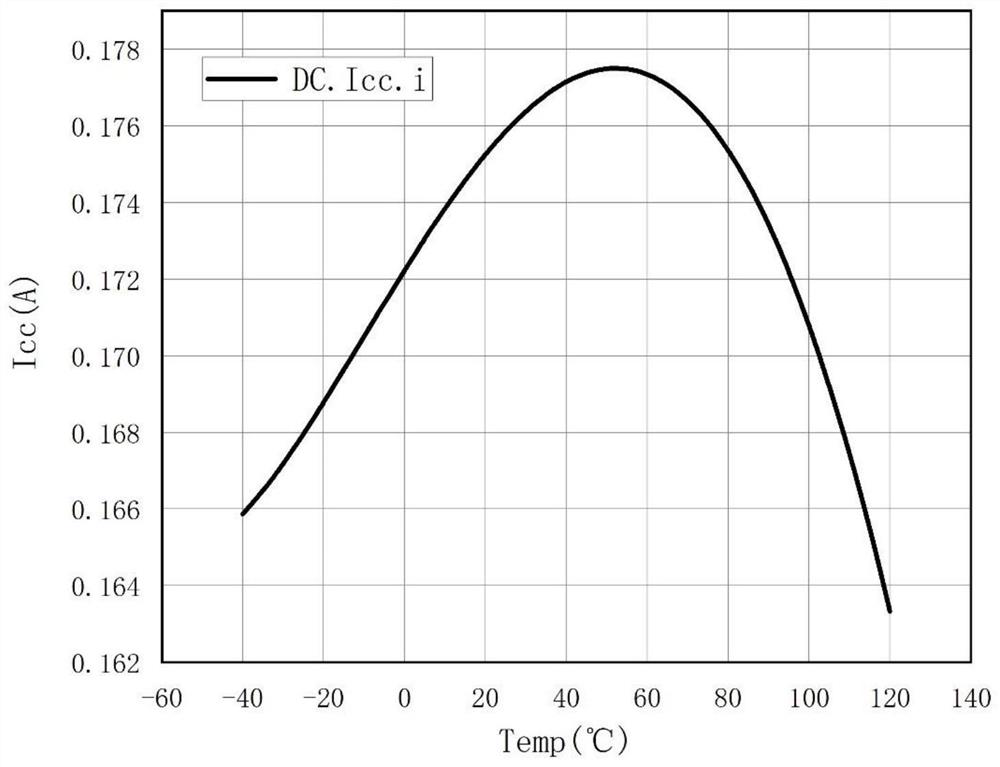
[0004] But for GaAs HBT, there is an obvious disadvantage: the device junction temperature rises and the emitter voltage drops due to the self-heating effect, which causes a sudden gain collapse
In this way, the originally set bias point will be shifted, causing the transconductance of the tube to change, and the gain compression will occur in advance
[00
Method used
View moreImage
Smart ImageViewing Examples

Examples
 PUM
 Abstract
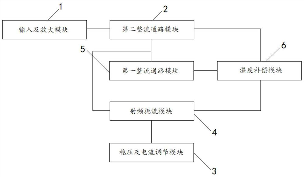
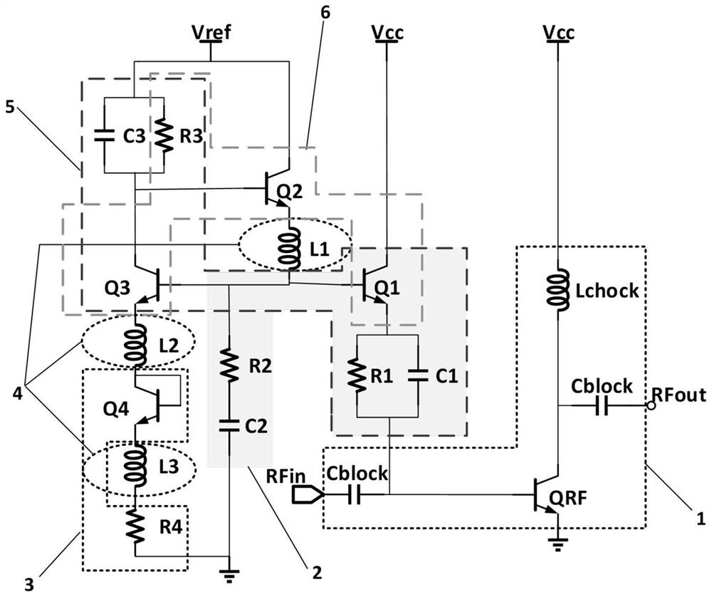
The invention discloses a biasing circuit for a radio frequency power amplifier, wherein the biasing circuit comprises an input and amplification module which is used for receiving an input radio frequency signal, amplifying the radio frequency signal and then providing the amplified radio frequency signal to an output end, and comprises a radio frequency power tube QRF for amplifying a radio frequency signal; a first rectification path module, which is used for compensating for gain compression in medium power; a second rectification path module which is used for compensating for gain compression in high power, wherein the first rectification path module comprises a transistor Q3, and the second rectification path module comprises a transistor Q1 shared by the first rectification path module; a voltage stabilization and current regulation module, which is used for keeping the conducting state of the transistor Q1 and adjusting the proportion of current distributed to the transistor Q1 and the transistor Q3; a radio frequency choke module which is used for blocking leakage of radio frequency signals; and a temperature compensation module that is used for inhibiting the increase of the collector current of the transistor Q1 caused by temperature rise.
Description
technical field [0001] The invention relates to the technical field of radio frequency integrated circuits, in particular to a bias circuit applied to radio frequency power amplifiers, capable of improving the gain flatness of radio frequency power amplifiers, and having a temperature compensation function. Background technique [0002] The RF power amplifier is at the final stage of the transmission chain, and its function is to amplify the power of the high-frequency modulated carrier signal, and radiate the signal into space through the antenna for long-distance transmission. Therefore, in order to ensure that the other party can receive the sender's information accurately in a certain area, certain requirements must be placed on the output power and linearity of the RF power amplifier, and the increasing update of information technology has continuously prompted the system to adjust the RF power. The performance requirements of amplifiers are getting higher and higher. ...
Claims
Login to View More Application Information
Patent Timeline
 IPC IPC(8): H03F1/30H03F3/189
CPCH03F1/30H03F3/189
Inventor陈建强张志浩林少鑫钟经智章国豪
OwnerGUANGDONG UNIV OF TECH