PCB solder mask plug hole base and manufacturing method of PCB solder mask plug hole base
A plug hole and anti-soldering technology, which is applied in the manufacture of printed circuits, the formation of electrical connections of printed components, electrical components, etc., can solve the problems of increasing costs, consuming large plates, and difficult processing of the base, so as to prolong the service life and save the amount of substrates , the effect of high strength and stiffness
- Summary
- Abstract
- Description
- Claims
- Application Information
AI Technical Summary
Problems solved by technology
Method used
Image

Examples
Example Embodiment
[0043] Embodiment one
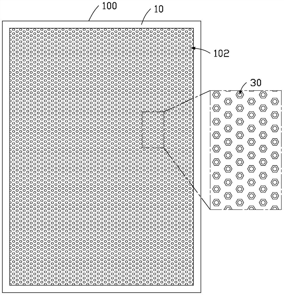
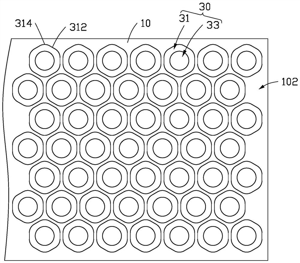
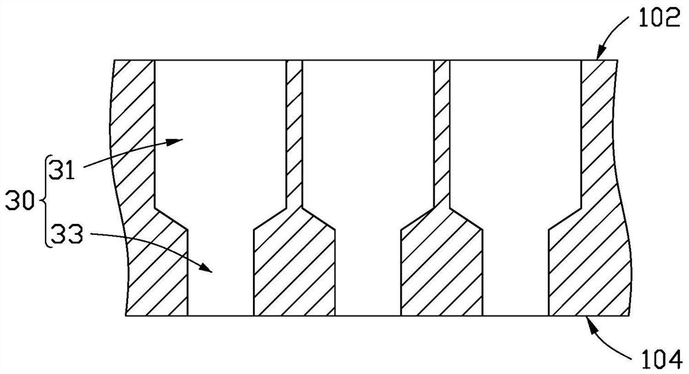
[0044] This embodiment provides a PCB anti-solder plug hole base, please refer to figure 1 The PCB anti-solder plug hole base 100 includes a substrate 10 and a plurality of spaced air guide through holes 30 opened on the substrate 10, and the plurality of air guide through holes 30 run through the opposite upper surface 102 and lower surface 104 of the substrate 10 ( ginseng image 3 ). Each air guiding through hole 30 is closely adjacent to the other six air guiding through holes 30 .
[0045] In this embodiment, the substrate 10 may be a stainless steel plate, a copper-clad laminate, etc., which are easy to clean and have high hardness, so as to facilitate repeated use and save costs.
[0046] In this embodiment, the thickness of the substrate 10 is 3 mm, so as to facilitate the opening of the air-conducting through holes 30 and save material costs. In other embodiments, the thickness of the substrate 10 may also be 2mm-3mm.
[0047] Please also ...
Example Embodiment
[0058] Embodiment two
[0059] This embodiment provides a PCB anti-solder plug hole base, please refer to Figure 5 The PCB anti-solder plug hole base 100 includes a substrate 10 and a plurality of spaced air guide holes 50 opened on the substrate 10 , and the plurality of air guide holes 50 penetrate the upper surface 102 and the lower surface 104 of the substrate 10 . Each air guiding through hole 50 is closely adjacent to the other six air guiding through holes, and a plurality of air guiding through holes are densely arranged to form a honeycomb structure.
[0060] In this embodiment, each air guide hole 50 includes a first air guide hole 51 and a second air guide hole 53 , the first air guide hole 51 penetrates the upper surface 102 of the substrate 10 , and the second air guide hole 53 penetrates the lower surface of the substrate 10 104 , and each first air guide hole 51 communicates with a second air guide hole 53 .
[0061] In this embodiment, both the first air gui...
Example Embodiment
[0066] Embodiment Three
[0067] The embodiment of the present application also provides a method for manufacturing a PCB anti-solder plug hole base, please refer to Figure 7 , the production method includes:
[0068] Step S1: providing a substrate;
[0069] Step S2: setting up a plurality of spaced first air guide holes on the substrate, the first air guide holes penetrate the upper surface of the substrate, and each of the first air guide holes is connected to the other six first air guide holes adjacent;
[0070] Step S3: setting up a plurality of spaced second air guide holes on the substrate, the second air guide holes penetrate the lower surface of the substrate, and communicate with the first air guide holes.
[0071] In one embodiment, the first air guide hole opened in step S2 is coaxial with the second air guide hole opened in step S3, and the first air guide hole and the second air guide hole can be opened on the same surface of the substrate, so as to ensure th...
PUM
| Property | Measurement | Unit |
|---|---|---|
| The inside diameter of | aaaaa | aaaaa |
| The inside diameter of | aaaaa | aaaaa |
Abstract
Description
Claims
Application Information
 - R&D Engineer
- R&D Manager
- IP Professional
- Industry Leading Data Capabilities
- Powerful AI technology
- Patent DNA Extraction
Browse by: Latest US Patents, China's latest patents, Technical Efficacy Thesaurus, Application Domain, Technology Topic.
© 2024 PatSnap. All rights reserved.Legal|Privacy policy|Modern Slavery Act Transparency Statement|Sitemap