
A nano-metal-assisted directional electroplating and electrolysis circuit forming and repairing method

A nano-metal and repair method technology, which is applied in printed circuit, printed circuit manufacturing, printed circuit secondary treatment, etc., can solve problems such as complex process, and achieve the effect of promoting diffusion, promoting diffusion and transport, and maintaining ion concentration

Active Publication Date: 2022-05-17
GUANGDONG UNIV OF TECH
View PDF4 Cites 0 Cited by
  • Summary
  • Abstract
  • Description
  • Claims
  • Application Information

AI Technical Summary

Problems solved by technology

[0005] Aiming at the forming and repairing of fine circuit boards, the present invention provides a precise and efficient nano-metal assisted directional electroplating and electrolytic circuit forming and repairing method, so as to effectively overcome the complex process and problems existing in the existing circuit forming and repairing methods. limitations

Method used


Image

  • A nano-metal-assisted directional electroplating and electrolysis circuit forming and repairing method
  • A nano-metal-assisted directional electroplating and electrolysis circuit forming and repairing method
  • A nano-metal-assisted directional electroplating and electrolysis circuit forming and repairing method

Examples


Embodiment 1

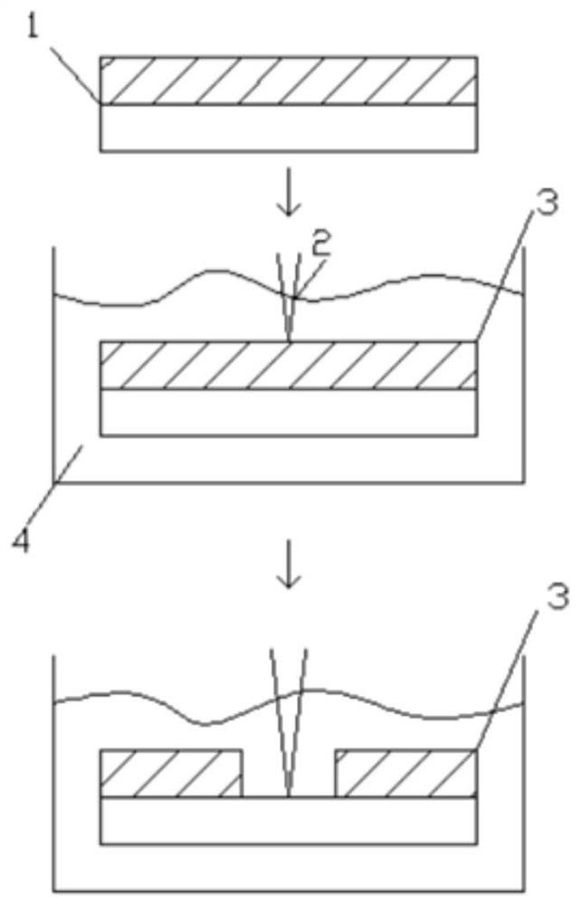
[0066] see figure 1 , for the 10×10mm copper circuit board 1 to be formed, the following steps are used for forming:

[0067] 1) Determine the area 3 to be formed on the copper circuit board according to the process requirements.

[0068] 2) Use the direct contact method of the energized wire to energize the copper circuit board 1, so that the copper circuit board 1 is positively charged as a whole.

[0069] 3) Place the energized copper circuit board 1 in the copper sulfate solution 4 with a mass fraction of 10%, so that the copper sulfate solution 4 completely immerses the copper circuit board 1 .

[0070] 4) Use a highly conductive metal probe 2 with a diameter of 50 μm to move to a distance of 100 μm directly above the area to be repaired on the circuit board 1, and apply negative electricity to the metal probe 2 to make the gap between the circuit board 1 and the probe 2 A potential difference of 3V is generated, and a local current is formed in the area of ​​the circui...

Embodiment 2

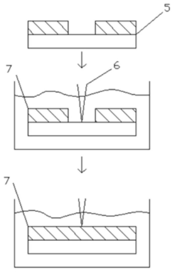
[0072] see figure 2 , for the rewiring layer copper circuit board 5 of 9x9mm to be repaired, the following steps are used to repair:

[0073] 1) Determine the position of the defect on the copper circuit board 5 by automatic optical detection technology, and determine the repair area 7 .

[0074] 2) Use the direct contact method of the energized wire to energize the copper circuit board 5, so that the copper circuit board 5 is negatively charged as a whole.

[0075] 3) Place the energized copper circuit board 5 in a copper chloride solution with a mass fraction of 7%, so that the solution completely immerses the copper circuit board 5 .

[0076] 4) Use a highly conductive metal probe 6 with a diameter of 30 μm to move to a distance of 100 μm directly above the area to be repaired on the circuit board 5, and apply positive electricity to the metal probe 6 to make the contact between the circuit board 5 and the probe 6 A potential difference of 5V is generated between them, a...

Embodiment 3

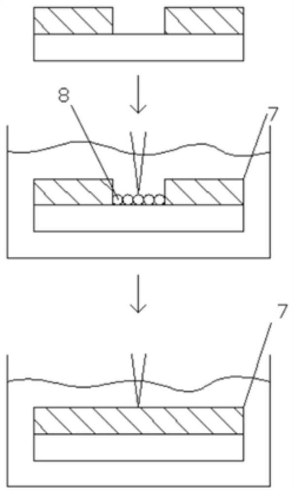
[0078] Embodiment 3 is substantially the same as Embodiment 2, except that Embodiment 3 also includes the following steps between steps 1) and 2):

[0079] Copper nanoparticles 8 coated with polyvinylpyrrolidone with a particle diameter of 50nm were added to ethylene glycol to form a copper paste with a solid content of 80% and sent to the defect position of the copper circuit board 7 through the drip nozzle.


PUM

PropertyMeasurementUnit
sizeaaaaaaaaaa

Abstract

The invention discloses a nano-metal-assisted directional electroplating and electrolysis circuit forming and repairing method, comprising: determining the area to be repaired on the metal circuit board to be repaired / determining the area to be formed on the metal circuit board to be formed, The circuit board is connected to electricity, and the negative electricity is connected when it is repaired, and the positive electricity is connected when it is formed; the metal circuit board after the electricity is immersed in the metal salt solution, and the metal probe is used to move to the top of the area to be repaired / formed. The needle is positively charged, and the metal probe is negatively charged during molding. The potential difference is used to reduce the metal salt to metal particles for repair, or electrolytically corrode the metal circuit board for molding. The invention localizes the electric field through the use of the thin probe, thereby realizing regional high-precision electroplating and electrolysis; the method helps to improve the forming efficiency and the utilization rate of the fine circuit board in the industry.

Description

technical field [0001] The invention relates to the technical field of integrated circuits, in particular to a nano-metal-assisted directional electroplating and electrolysis circuit forming and repairing method. Background technique [0002] Fine circuit board is the support body of electronic components and the carrier of electrical connection. With the development of electronic products towards miniaturization and digitization, printed circuit boards are also moving towards high density, high precision, fine aperture, thin wire, and fine pitch. High reliability, multi-layer, high-speed transmission, light weight, and thin profile development, put forward higher requirements for the forming and repair of fine lines. [0003] The commonly used method for forming fine circuits is to use graphic electroplating for circuit production. First, it is necessary to make preset circuit pattern grooves. After the circuit electroplating is completed, steps such as stripping and etchin...

Claims


Application Information

Patent Timeline
Patent Type & Authority Patents(China)
IPC IPC(8): H05K3/22H05K3/18C25D7/00C25D5/06
CPCH05K3/18H05K3/22C25D5/06C25D7/00Y02W30/82
Inventor 杨冠南吴润熹崔成强张昱
Owner GUANGDONG UNIV OF TECH
Learn More