Side-emission typy LED package

a technology of led package and light-emitting diodes, which is applied in the direction of semiconductor devices for light sources, light-emitting devices, refractors, etc., can solve the problems of difficult manufacturing of led lens b>10/b>, deterioration of optical characteristics of led package, etc., and achieve the effect of improving manufacturing efficiency and improving molding efficiency of sealing members

Active Publication Date: 2006-08-03
SAMSUNG ELECTRONICS CO LTD
View PDF8 Cites 26 Cited by
  • Summary
  • Abstract
  • Description
  • Claims
  • Application Information

AI Technical Summary

Benefits of technology

[0013] An object of the present invention is to provide a side-emission type LED package capable of improving molding efficiency of a sealing member and thus improving manufacturing efficiency by separately providing a lower structure for reflecting light upward from an LED chip and an upper structure for reflecting the light in a lateral direction and combining the lower and the upper structures.

Problems solved by technology

However, the related art LED lens 10 has the following problems.
First, the LED lens 10 is difficult to manufacture.
However, there still exists possibility that the bubbles might remain despite the additional process, which might deteriorate optical characteristics of the LED package.

Method used


Image

  • Side-emission typy LED package
  • Side-emission typy LED package
  • Side-emission typy LED package

Examples


fourth embodiment

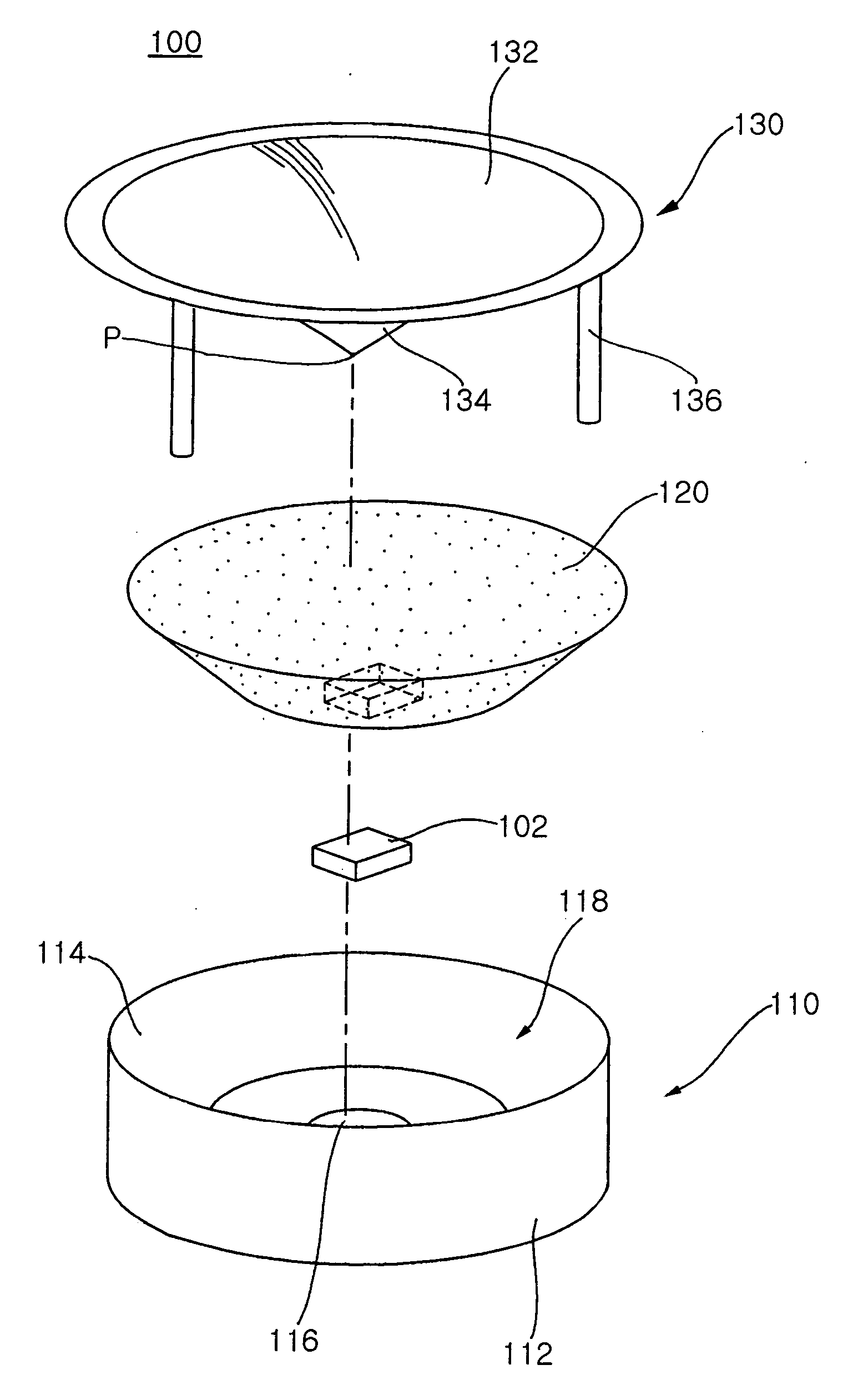
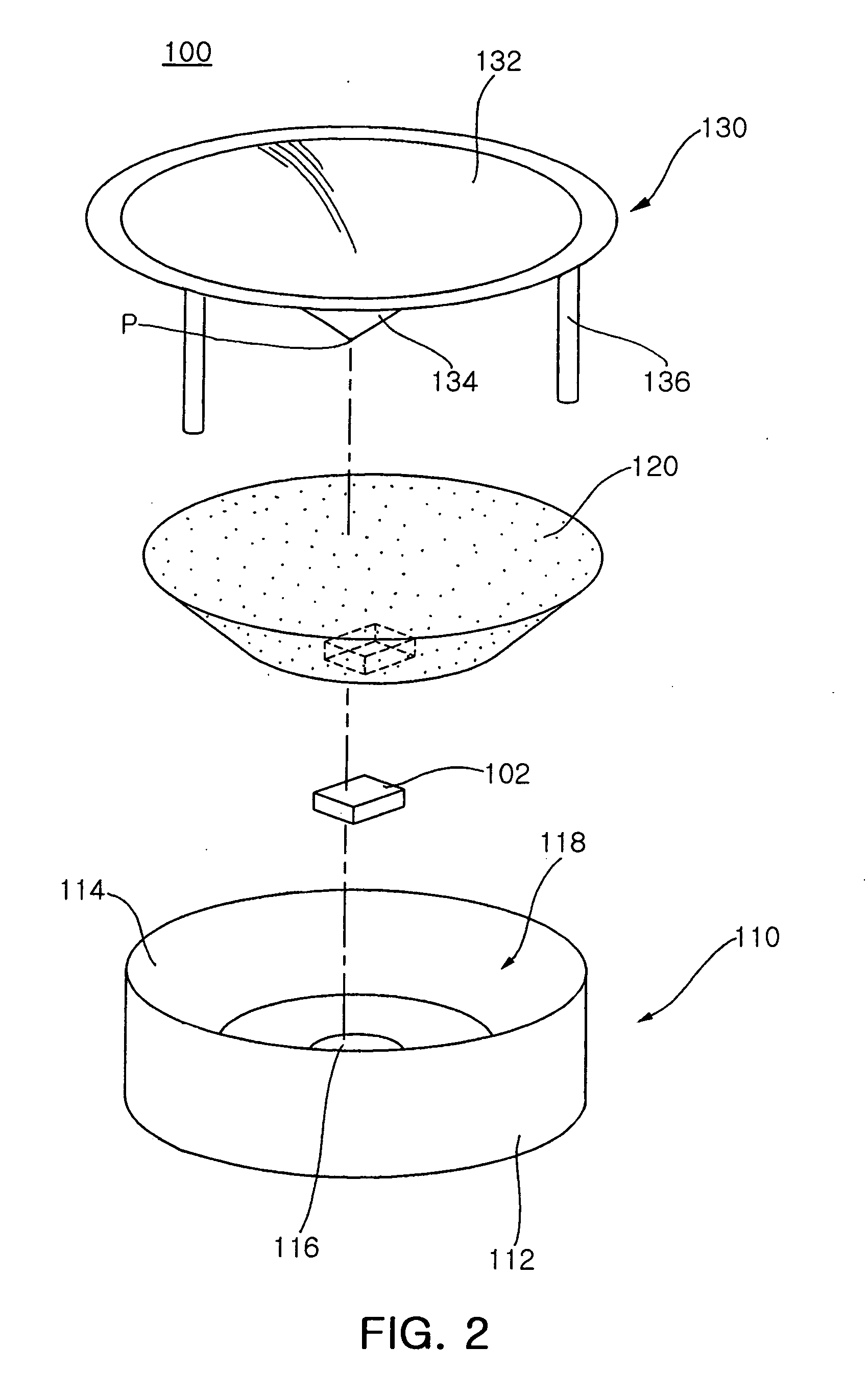
[0105]FIG. 10 is a cross-sectional view of an LED package according to the present invention and FIG. 11 is a schematic, cross-sectional view illustrating an operation of the LED package of FIG. 10.

[0106] Referring to FIG. 10, an LED package 400 of the fourth embodiment is the same as the LED package 300 of the third embodiment except that a sealing member 420 formed around an LED chip 402 inside a concaved cavity C is of a hemisphere shape having a predetermined radius r, part of the cavity C is maintained vacant, and a bottom of the upper structure 430 is combined to an upper edge of a lower structure 410. Therefore, the same reference numerals starting with 400 are given to the corresponding elements and descriptions thereof are omitted.

[0107] The sealing member 420 can be formed in a variety of shapes including a hemisphere, a dome, an ellipse, a frustum such as a truncated dome and a structure in which the cavity C of the lower structure 410 is filled only around the LED chip ...

third embodiment

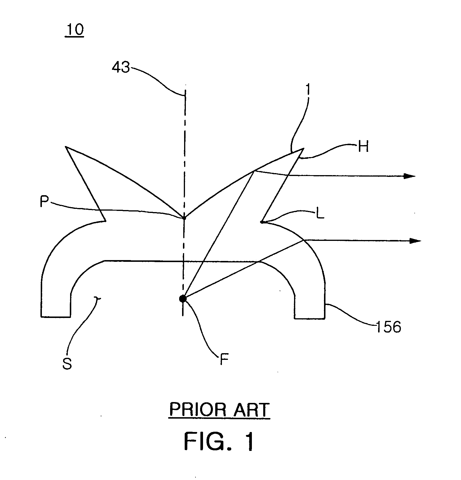
[0111] Referring to FIG. 11, an optical path I1 represents light propagating from the focus F of the LED chip to a connection point P1 at an edge of the lower mirror 414, an optical path I2 represents light propagating from the focus F of the LED chip to a connection point P2 between the reflecting surface 434 and the discharging surface 436. In case of the LED package 300 of the third embodiment, light between the optical paths I1 and I2 is all directly discharged through the discharging surface 436 without passing through the reflecting surface 434.

[0112] However, since the sealing member 420 is of a hemisphere shape and a vacant space is formed in a cavity C between the sealing member 420 and the bottom 438 of the upper structure 430 according to the fourth embodiment, light L1 and Lx generated from the focus F propagates straight when coming from the sealing member 420 but is refracted toward the reflecting surface 434 by a difference in the refractive indexes between air and th...

fifth embodiment

[0113]FIG. 12 is a perspective view of LED assembly according the invention, FIG. 13 is a front elevational view of the LED assembly shown in FIG. 12, and FIG. 14 is a cross-sectional view of the LED assembly shown in FIG. 12.

[0114] Referring to FIGS. 12 to 14, an LED assembly 500 of this embodiment is arranged on a substrate, which is preferably a reflector plate inside a backlight unit (not shown). Each LED assembly 500 part includes an LED chip 502, a lower structure 510 seated on the board 540 and an upper structure 530, and arranged at a predetermined interval from adjacent assembly parts. The lower structure 510 is designed to seat the LED chip 502 thereon while reflecting light upward from the LED chip 502, and the upper structure 530 is designed to reflect light from the lower structure substantially radially in a lateral direction.

[0115] The lower structure 510 has a body 512 housing the LED chip 502, and a central portion of the body 512 is concaved downward forming a cav...


PUM


Abstract

A side-emission type LED package is provided. The LED package includes an LED chip, a lower structure, and an upper structure. The lower structure has a lower mirror and a transparent sealing member. The lower structure supports the LED chip. The lower mirror is extended upward and outward@ from the LED chip so as to reflect light from the LED chip upward. The transparent sealing member is formed around the LED chip inside the lower mirror. The upper structure is combined to an upper portion of the lower structure so as to reflect the light reflected upward by the lower structure to a radial lateral direction. As described above, the lower structure and the upper structure are separately provided and combined with each other, whereby molding efficiency of the sealing member is improved and the side-emission type LED package can be manufactured in an easy manner.

Description

RELATED APPLICATION [0001] The present application is based on, and claims priority from, Korean Application Numbers 10-2005-0010046, filed Feb. 3, 2005, and 10-2005-0044649, filed May 26, 2005, the disclosure of which is hereby incorporated by reference herein in its entirety. BACKGROUND OF THE INVENTION [0002] 1. Field of the Invention [0003] The present invention relates to a side-emission type light-emitting diode (LED) package, and more particularly, to a side-emission type LED package capable of improving molding efficiency of a sealing member by separately providing a lower structure for reflecting light upward from an LED chip and an upper structure for reflecting the light in a lateral direction and then combining the lower and the upper structures. [0004] 2. Description of the Related Art [0005] As the electronic apparatus industry develops, a liquid crystal display (LCD) is drawing attention as a next-generation display device. Since the LCD does not emit light spontaneou...

Claims


Application Information

Patent Timeline
Patent Type & Authority Applications(United States)
IPC IPC(8): F21V5/00F21V7/09H01L33/56F21V7/22H01L33/60
CPCF21K9/00H01L33/54H01L33/60F21K9/68
Inventor PARK, YOUNG SAMKIM, HYUNG SUKPARK, JUNG KYUAHN, HO SIKJEONG, YOUNG JUNEHAHM, HUN JOOKIM, BUM JIN
Owner SAMSUNG ELECTRONICS CO LTD
Why Eureka
Try Eureka