PCB correction equipment and correction method thereof

A PCB board and equipment technology, applied in the field of PCB board correction equipment, can solve problems such as secondary deformation, PCB board deformation, PCB board production process complexity, etc., to reduce processing time, high production efficiency, and realize semi-automatic production processing Effect

Active Publication Date: 2021-08-03
广东兴达鸿业电子有限公司
View PDF6 Cites 2 Cited by
  • Summary
  • Abstract
  • Description
  • Claims
  • Application Information

AI Technical Summary

Problems solved by technology

The production process of PCB boards is complicated and needs to be washed and dried many times. Due to improper process or human operation, PCB boards are easy to be deformed. Existing manufacturers generally use direct scrapping or manual repair with hot air guns. Direct scrapping will lead to direct economic losses. The effect of manual repair is poor, prone to secondary deformation

Method used


Image

  • PCB correction equipment and correction method thereof
  • PCB correction equipment and correction method thereof
  • PCB correction equipment and correction method thereof

Examples


Embodiment Construction

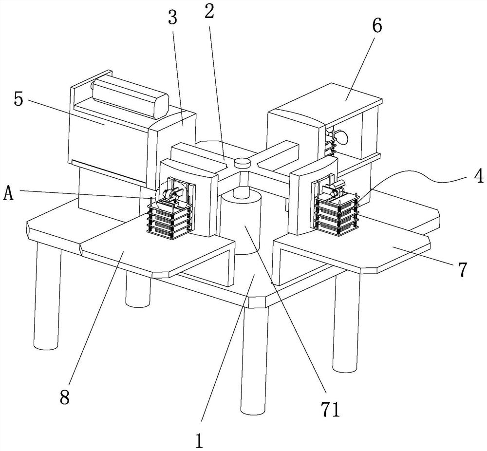
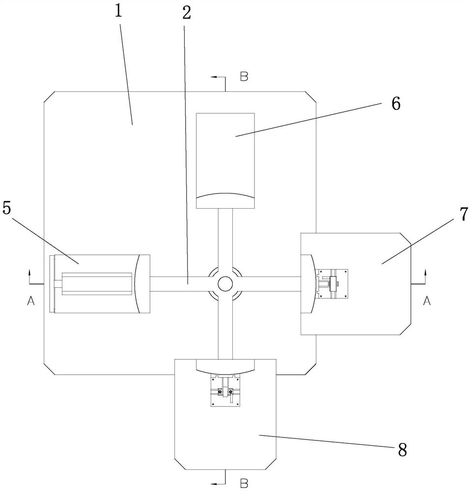
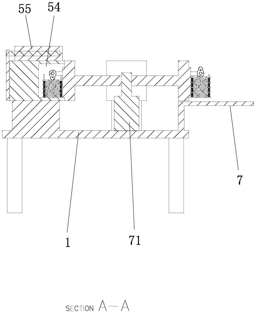
[0028] The following detailed description provides various embodiments or examples for implementing the invention. Of course, these are merely embodiments or examples and are not intended to be limiting. In addition, repeated reference numerals, such as repeated numbers and / or letters, may be used in different embodiments. These repetitions are for the purpose of simply and clearly describing the present invention, and do not represent any specific relationship between the different embodiments and / or structures discussed.

[0029] In addition, terms related to space may be used, such as "below", "underside", "inside out", "above", "upper side" and similar terms, these relative words To facilitate describing the relationship between one element or feature and another element or feature in the drawings, these spatial relative terms include different orientations of the device in use or operation, as well as the orientation depicted in the drawings. The device may be turned to...


PUM


Abstract

The invention discloses a PCB correction device and a correction method thereof. A rotating mechanism and a rotating frame installed on the rotating mechanism are arranged on a workbench, four fixed installation plates are arranged on the rotating frame in a circumferential array mode with the rotating mechanism as the circle center, and extrusion assemblies used for pressing a PCB are arranged on the outer sides of the fixed installation plates; a heating device, a cooling device, a dismounting and mounting workbench and an assembling workbench are sequentially arrayed on the workbench with the rotating mechanism as the circle center along the circumference, and the extrusion assembly comprises a fixed bottom plate arranged below a fixed mounting plate and a vertical rail arranged on the outer side. A plurality of heat transfer steel plates are arranged in the vertical track in a sliding mode, an extrusion area used for containing a PCB is formed between every two adjacent heat transfer steel plates. The PCB correction equipment is high in production efficiency, semi-automatic production treatment can be achieved, the machining time is shortened, and meanwhile, the correcting rate reaches up to 99% or above.

Description

technical field [0001] The invention relates to the technical field of PCB board processing, in particular to a PCB board straightening device and a straightening method thereof. Background technique [0002] PCB (Printed Circuit Board), the Chinese name is a printed circuit board, also known as a printed circuit board, is an important electronic component, a support for electronic components, and a carrier for the electrical connection of electronic components. Developed to double-sided, multi-layer and flexible, and still maintain their own development trends. The production process of PCB boards is complicated and needs to be washed and dried many times. Due to improper process or human operation, PCB boards are easy to be deformed. Existing manufacturers generally use direct scrapping or manual repair with hot air guns. Direct scrapping will lead to direct economic losses. The effect of manual repair is poor, and secondary deformation is prone to occur. In view of the ...

Claims


Application Information

Patent Timeline
Patent Type & Authority Applications(China)
IPC IPC(8): H05K3/22
CPCH05K3/225
Inventor 郑小红胡泽洪梁锐玲何旭谢斌
Owner 广东兴达鸿业电子有限公司
Why Eureka
Try Eureka