A structure optimization design method of to packaged power semiconductor device

A power semiconductor and optimization design technology, applied in the field of TO package power semiconductor device structure optimization design, can solve problems such as hindering the application of engineering optimization algorithms, and achieve the effect of easy understanding, good applicability, and clear steps

Active Publication Date: 2022-04-12
HUNAN CITY UNIV
View PDF0 Cites 0 Cited by
  • Summary
  • Abstract
  • Description
  • Claims
  • Application Information

AI Technical Summary

Problems solved by technology

Thus, it greatly hinders the application of engineering optimization algorithms in the structural design of power semiconductor devices

Method used


Image

  • A structure optimization design method of to packaged power semiconductor device
  • A structure optimization design method of to packaged power semiconductor device
  • A structure optimization design method of to packaged power semiconductor device

Examples


Embodiment Construction

[0056] Below in conjunction with embodiment, the present invention is described further, but does not constitute any restriction to the present invention, any limited number of modifications done in the scope of claims of the present invention is still within the scope of claims of the present invention.

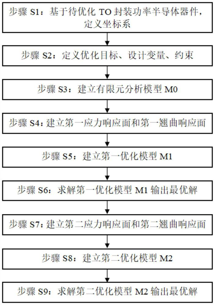
[0057] Such as figure 1 — image 3 As shown, the present invention provides a method for structural optimization design of a TO package power semiconductor device, the method comprising the following processing steps:

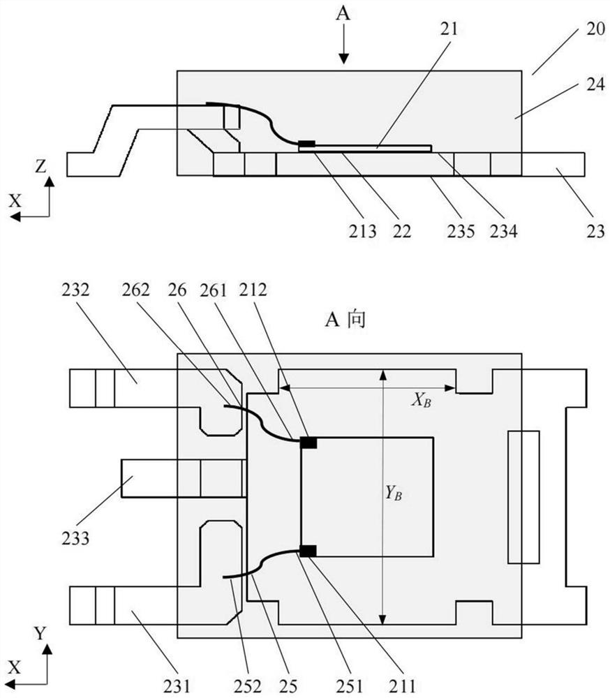
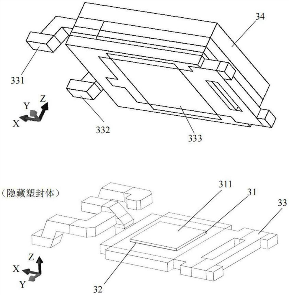
[0058] Step 1: Define the coordinate system based on the TO package power semiconductor device to be optimized. Such as figure 2 As shown, the package model of the TO package power semiconductor device 20 to be optimized is TO-252, including a chip 21 , a solder layer 22 , a lead frame 23 , a plastic package 24 , a first bonding wire 25 , and a second bonding wire 26 . The lower surface 213 of the chip is connected to the upper surface 234 of the base of ...


PUM


Abstract

The invention relates to the technical field of power semiconductor devices, discloses a structure optimization design method for a TO package power semiconductor device, and aims to provide a practical design tool for the structure optimization of a TO package power semiconductor device. This method first defines the optimization objectives, design variables and constraints of the power semiconductor device to be optimized; secondly, a finite element analysis model is established to analyze the thermal stress and warpage of the chip in the device; thirdly, combined with response surface technology, two The structure optimization model optimizes the chip structure size and position size in turn. Compared with the existing technology, this method sequentially optimizes the chip structure size and position size, which can minimize the chip warpage and meet the constraints of thermal stress and chip area; the steps are clear and easy to understand, and can be directly used to solve the power consumption of general TO packages. The structural design of semiconductor devices has good ease of use and applicability.

Description

technical field [0001] The invention relates to the technical field of power semiconductor devices, in particular to a structure optimization design method for a TO package power semiconductor device. Background technique [0002] Power semiconductor devices use switches in power electronic systems to efficiently convert electric energy in the switch network, thereby achieving high-precision and high-reliability transmission of energy. Power semiconductor devices have become semiconductor devices widely used in power electronic system control circuits and power conversion. Discrete packaging is one of the main packaging structures of power semiconductor devices, and Transistor Outline (TO) packaging is the most widely used discrete packaging structure. The TO package is sealed by a plastic package, and the chip inside the plastic package is directly welded on the copper-based lead frame. One end of the bonding wire is welded to the lead frame, and the other end is led to th...

Claims


Application Information

Patent Timeline
Patent Type & Authority Patents(China)
IPC IPC(8): G06F30/23
CPCG06F30/23
Inventor 黄志亮邓洁莲邓曙光阳同光李航洋陈敢新
Owner HUNAN CITY UNIV
Why Eureka
Try Eureka