Wafer storage box

A storage box and wafer technology, applied in packaging, external frame, bottle/can components, etc., can solve the problems of inability to guarantee the accuracy of wafer placement, misplacement of wafer storage boxes, etc., to improve the accuracy of wafer placement and storage efficiency, avoiding the effect of mis-insertion problems

Active Publication Date: 2021-08-27
JITRI INST OF ORGANIC OPTOELECTRONICS CO LTD
View PDF12 Cites 2 Cited by
  • Summary
  • Abstract
  • Description
  • Claims
  • Application Information

AI Technical Summary

Problems solved by technology

[0003] For this reason, the technical problem to be solved by the present invention is to overcome the problem that the wafer storage box in the prior art is prone to mis-insertion and cannot guarantee the accuracy of film placement.

Method used


Image

  • Wafer storage box
  • Wafer storage box
  • Wafer storage box

Examples


Embodiment 1

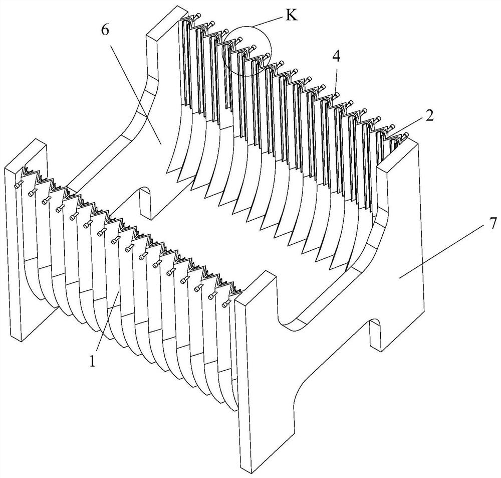
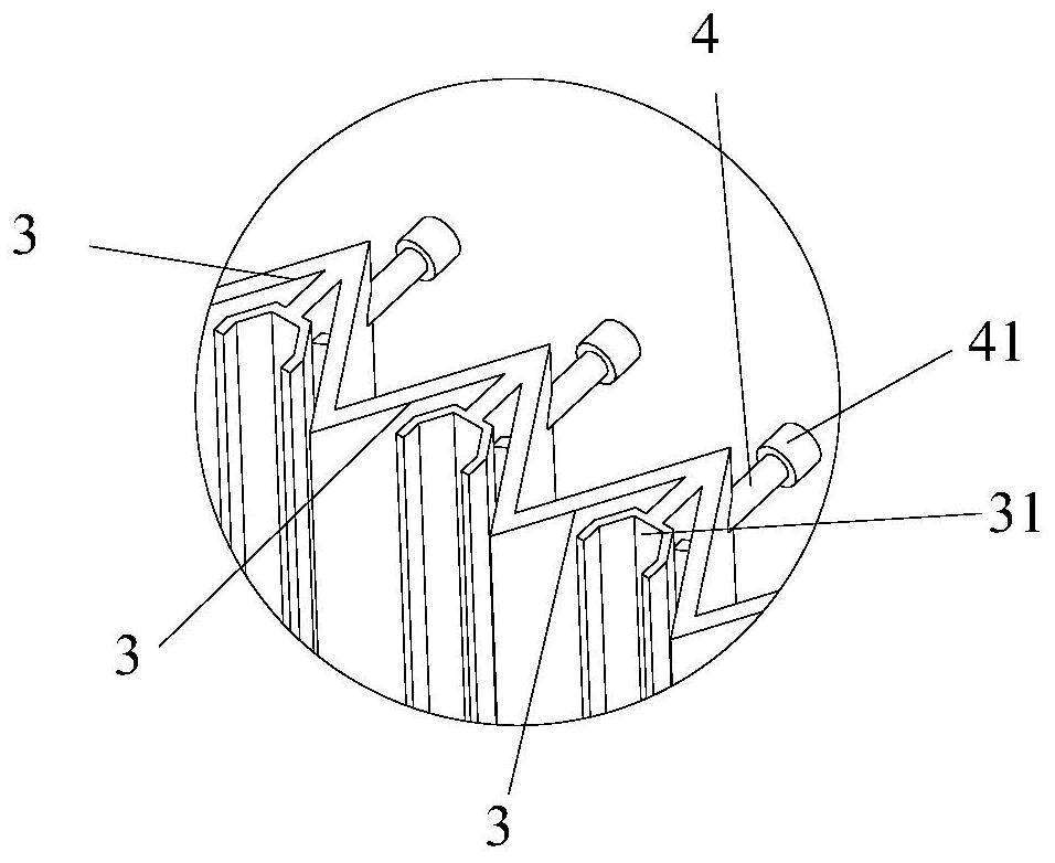
[0029] refer to Figure 1-Figure 2 As shown, the present invention discloses a wafer storage box, comprising a first telescopic board 1 and a second telescopic board 2, and a plurality of folding grooves 3 are formed on the first telescopic board 1 and the second telescopic board 2, the first The folding slots on the telescopic board 1 correspond to the folding slots 3 on the second telescopic board 2 one by one, and the storage wafers are formed between the folding slots 3 on the first telescopic board 1 and the corresponding folding slots 3 on the second telescopic board 2 The outer wall of each folding groove 4 is connected with a push-pull rod 4, the first end of the push-pull rod 4 passes through the folding groove 3 and is connected with a support member 33, and one end of the support member 33 is hinged on the first end of the push-pull rod 4 One end and the other end are hinged on the inner wall of the folding groove 4 .

[0030] Through the setting of the support mem...

Embodiment 2

[0043] The difference between this embodiment and Embodiment 1 is:

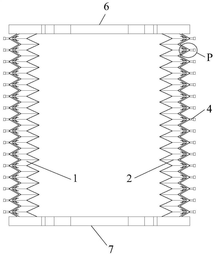
[0044] refer to Figure 6 , Figure 7 and Figure 9, the bottom of the locator 31 in the corresponding folding groove 3 of the first telescopic plate 1 and the second telescopic plate 2 is connected by a U-shaped slot 5, and the groove shape of the U-shaped slot 5 is compatible with the locator 31. For example, if the shape (cross section) of the positioning member 31 is V-shaped, then the groove body shape (cross section) of the U-shaped locking groove 5 is also V-shaped. Since the telescopic plate stretches and contracts, it will exert a slight force on the placed wafer to make it move, and the wafer is easily squeezed and damaged during the moving process. In order to avoid the above phenomenon, the above-mentioned U-shaped slot 5 is designed so that the The round bottom can be supported in the above-mentioned U-shaped groove 6 , so that the entire wafer can be fixed, and it is not easy to fall or be da...


PUM


Abstract

The invention relates to a wafer storage box which comprises a first telescopic plate and a second telescopic plate. Multiple folding grooves are formed in the first telescopic plate and the second telescopic plate, the folding grooves in the first telescopic plate are in one-to-one correspondence to the folding grooves in the second telescopic plate, storage cavities for storing wafers are formed between the folding grooves in the first telescopic plate and the corresponding folding grooves in the second telescopic plate, the outer wall of each folding groove is connected with a push-pull rod, the first end of each push-pull rod penetrates through the corresponding folding groove and is connected with a supporting piece, one end of each supporting piece is hinged to the first end of the corresponding push-pull rod, and the other end of each supporting piece is hinged to the inner wall of the corresponding folding groove. According to the wafer storage box, the problem of wrong insertion during wafer placement can be effectively avoided, and the wafer placement accuracy and the storage efficiency are greatly improved.

Description

technical field [0001] The invention relates to the technical field of wafer storage, in particular to a wafer storage box. Background technique [0002] Wafer refers to the silicon wafer used in the production of silicon semiconductor integrated circuits. Because of its circular shape, it is called a wafer. It can be processed into various circuit element structures on the silicon wafer and become an IC with specific electrical functions. product. In order to ensure the safe storage, transportation and handling of wafers, wafer storage boxes are widely used as wafer carrying and transportation tools. The wafer storage box is composed of multiple storage compartments, but the storage compartments inside the existing wafer storage box are narrow in size and densely arranged, which is not convenient for accurately inserting the wafer into the corresponding storage compartment. The problem of staggered insertion is prone to occur, which affects the accuracy of wafer placement...

Claims


Application Information

Patent Timeline
Patent Type & Authority Applications(China)
IPC IPC(8): B65D25/10B65D61/00
CPCB65D25/107B65D61/00
Inventor 廖良生王金彬朱凯祝晓钊冯敏强
Owner JITRI INST OF ORGANIC OPTOELECTRONICS CO LTD
Why Eureka
Try Eureka