Array substrate and display device
A technology of array substrate and substrate substrate, which is applied in static indicators, optics, instruments, etc., can solve the problems of poor display effect of liquid crystal display panels
- Summary
- Abstract
- Description
- Claims
- Application Information
AI Technical Summary
Problems solved by technology
Method used
Image

Examples
Embodiment Construction
[0040] In order to make the purpose, technical solution and advantages of the present application clearer, the implementation manners of the present application will be further described in detail below in conjunction with the accompanying drawings.
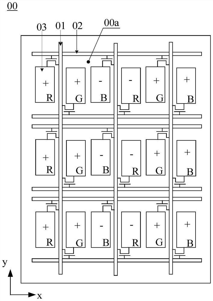
[0041] Please refer to figure 1 , figure 1 It is a structural schematic diagram of an array substrate prepared by adopting a double gate line technology provided by the related art. The array substrate 00 may include: a plurality of data lines 01 , a plurality of gate lines 02 and a plurality of sub-pixels 03 , the gate lines 02 extend along a first direction x, and the data lines 01 extend along a second direction y. The data lines 01 and the gate lines 02 can define a plurality of pixel areas 00a, and two sub-pixels 03 are arranged in each pixel area 00a along the first direction x. The plurality of pixel areas 00a may be arranged in multiple rows along the first direction x, and may also be arranged in multiple columns along...
PUM
 Abstract
Description
Claims
Application Information
 - R&D
- Intellectual Property
- Life Sciences
- Materials
- Tech Scout
- Unparalleled Data Quality
- Higher Quality Content
- 60% Fewer Hallucinations
Browse by: Latest US Patents, China's latest patents, Technical Efficacy Thesaurus, Application Domain, Technology Topic, Popular Technical Reports.
© 2025 PatSnap. All rights reserved.Legal|Privacy policy|Modern Slavery Act Transparency Statement|Sitemap|About US| Contact US: help@patsnap.com