Integrated circuit welding spot detection method

A solder joint detection and integrated circuit technology, which is applied to measurement devices, material analysis by optical means, instruments, etc., can solve the problems that the detection equipment cannot detect circuit boards of different sizes, the degree of automation is not high, and the floor space is large. Achieve the effect of high degree of automation, high detection efficiency and small floor space

Inactive Publication Date: 2021-09-17
安徽芯鑫半导体有限公司
View PDF0 Cites 5 Cited by
  • Summary
  • Abstract
  • Description
  • Claims
  • Application Information

AI Technical Summary

Problems solved by technology

[0003] The purpose of the present invention is to provide a method for detecting solder joints of integrated circuits, which solves the following technical problems: (1) solves the problem that the circuit board detection equipment in the prior art occupies a large space, and at the same time, the operator needs to place the circuit board at the detection position during detection , the technical problem of low degree of automation; (2) solve the technical problem that the detection equipment in the prior art cannot comprehensively detect circuit boards of different sizes

Method used


Image

  • Integrated circuit welding spot detection method
  • Integrated circuit welding spot detection method
  • Integrated circuit welding spot detection method

Examples


Embodiment Construction

[0027] The following will clearly and completely describe the technical solutions in the embodiments of the present invention with reference to the accompanying drawings in the embodiments of the present invention. Obviously, the described embodiments are only some, not all, embodiments of the present invention. Based on the embodiments of the present invention, all other embodiments obtained by persons of ordinary skill in the art without creative efforts fall within the protection scope of the present invention.

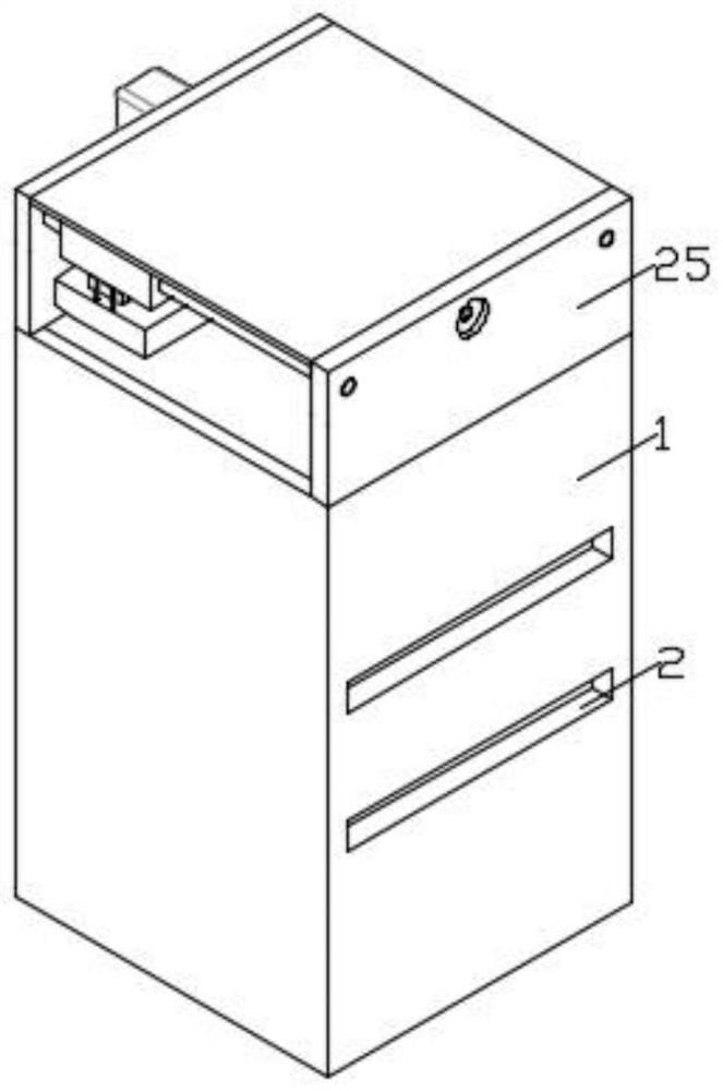
[0028] see Figure 1-9 As shown, the present invention is a method for detecting solder joints of integrated circuits, comprising the following steps:

[0029] Step 1: insert the circuit board to be tested into the board inlet 2 of the detection chamber 1 in the testing equipment, put the circuit board on the board feeding mechanism 8, turn on the conveying motor 11, and the output shaft of the conveying motor 11 drives the belt roller 12 to rotate, Two belt rolle...


PUM


Abstract

The invention discloses an integrated circuit welding spot detection method, which comprises the following steps of: inserting a to-be-detected circuit board into a board inlet of a detection chamber in detection equipment, putting the circuit board on a board conveying mechanism, adjusting the position of the circuit board above a bottom plate by a conveying belt, driving the board conveying mechanism to circularly lift by two mounting chains through a first side plate and a second side plate, and driving the to-be-detected circuit board to ascend to the top by the board conveying mechanism. According to the invention, the arrangement of the board conveying mechanism can ensure that the circuit board can automatically and horizontally enter and exit from the detection chamber so as to achieve high automation degree, and the position of the circuit board on the bottom plate can be adjusted, so that manual adjustment is not needed; the detection equipment can cyclically and sequentially detect the circuit board, so that the detection efficiency is high; and the floor space occupied by the whole detection equipment is small, circuit boards of different sizes can be clamped through the limiting mechanism, the distance between the detection camera and the circuit board can be conveniently adjusted through the arrangement of an air cylinder installed on the detection mechanism, and the detection camera can conveniently shoot and detect welding spots on the circuit board.

Description

technical field [0001] The invention relates to the technical field of circuit board detection, in particular to a method for detecting solder joints of an integrated circuit. Background technique [0002] An integrated circuit is a tiny electronic device or component. Using a certain process, the transistors, resistors, capacitors, inductors and other components required in a circuit are interconnected, and they are fabricated on a small or several small semiconductor wafers or dielectric substrates, and then packaged in a tube. , into microstructures with desired circuit functions. During circuit board processing, it is usually by soldering electrical components on the circuit board. Usually after soldering, it is necessary to inspect the solder joints. The existing inspection equipment cannot detect the solder joints on circuit boards of different sizes. The incomplete detection of solder joints affects the use of subsequent circuit boards, and the entire inspection pro...

Claims


Application Information

Patent Timeline
Patent Type & Authority Applications(China)
IPC IPC(8): G01N21/01G01N21/892
CPCG01N21/01G01N21/892
Inventor 周蔚
Owner 安徽芯鑫半导体有限公司
Why Eureka
Try Eureka