Flip chip space pixel arrangement structure and display panel device

A pixel arrangement, flip-chip technology, applied in electrical components, electric solid-state devices, circuits, etc., can solve problems such as difficulty in meeting high-resolution, high-brightness requirements, inability to increase pixel density, and difficulty in color mixing and matching. , to reduce the average physical cost, avoid pixel graininess, and improve the effect of pixel color mixing

Active Publication Date: 2021-09-17
SHENZHEN LAMP VIDEO TECH CO LTD
View PDF9 Cites 2 Cited by
  • Summary
  • Abstract
  • Description
  • Claims
  • Application Information

AI Technical Summary

Problems solved by technology

However, the distance between two adjacent pixels is much larger than the distance between internal sub-pixels, which will cause obvious graininess
This method is difficult to meet the high-resolution and high-brightness requirements of electronic equipment and high-definition image signal sources for display screens
[0006] related technologies, such as figure 2 As shown, in the existing LED-COB display screen pixels, one red sub-pixel, two green sub-pixels and one blu

Method used


Image

  • Flip chip space pixel arrangement structure and display panel device
  • Flip chip space pixel arrangement structure and display panel device
  • Flip chip space pixel arrangement structure and display panel device

Examples


Embodiment Construction

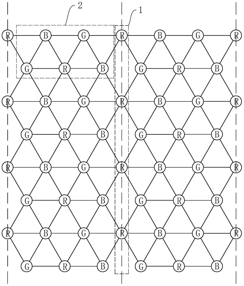
[0045] The following is attached Figure 3-7 , to further describe this application in detail.

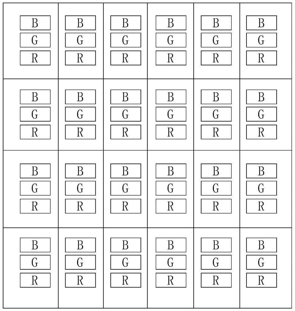
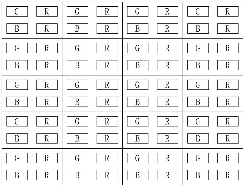
[0046] The embodiment of the present application discloses a flip-chip spatial pixel arrangement structure, which is used in the field of micro-LED or mini-LED self-luminous display. refer to image 3 , the pixel arrangement structure is divided according to the driving relationship, including a plurality of first pixel sets 1 and a plurality of second pixel sets 2, wherein the first pixel set 1 includes a number of A pixels arranged continuously, due to the different types of substrates and products Different, in some embodiments, the first pixel set 1 can be arranged in a single row of curves, in other embodiments, the first pixel set 1 can be arranged in a single row of straight lines, only two adjacent sets of first pixel sets 1. Parallel to each other or coincident in translation.

[0047] refer to image 3 and Figure 4 There are multiple second pixel sets 2 and they are...


PUM


Abstract

The invention relates to a flip chip space pixel arrangement structure and a display panel device.The flip chip space pixel arrangement structure comprises a plurality of first pixel sets and a plurality of second pixel sets, each first pixel set comprises a plurality of first pixels which are continuously arranged, each second pixel set comprises a central sub-pixel, and a pixel A, a pixel B, a pixel C, a pixel B and a pixel C which take the central sub-pixel as a circle center and are sequentially distributed on a semicircular arc, the pixel A, the pixel B and the pixel C are respectively one of a red light sub-pixel, a green light sub-pixel and a blue light sub-pixel, three independent white light spots are formed in each second pixel set, and each independent white light spot is formed by matching the central sub-pixel with any adjacent pixel on the corresponding semicircle; and the first pixel set and the second pixel set are independently and electrically controlled so as to control the on-off sequence and the on-off frequency of the independent white light spots. The display panel has the effects of improving the pixel density of the display panel and reducing the pixel granular sensation.

Description

technical field [0001] The present application relates to the field of self-luminous display field, in particular to a flip-chip spatial pixel arrangement structure and a display panel device. Background technique [0002] In flat panel display technology, Micro (Mini) inorganic light-emitting diode (LED) displays are widely used in the industry due to their thinness, active light emission, fast response speed, wide viewing angle, rich colors, high brightness, low power consumption, and high and low temperature resistance. It is recognized as the fourth-generation display technology after LCD displays, OLED displays, and LED billboards. Therefore, large-size, high-resolution panels can be realized, which is the focus of current research and the development direction of future display technology. [0003] With the development of display technology, people have higher and higher requirements for the resolution and brightness of the display screen. For high-resolution display ...

Claims


Application Information

Patent Timeline
IPC IPC(8): H01L27/15H01L33/48
CPCH01L27/156H01L33/48
Inventor 戴志明曾银海张鹏
Owner SHENZHEN LAMP VIDEO TECH CO LTD
Why Eureka
Try Eureka