Method for improving electrical testing efficiency of PCB
A technology of efficiency and electrical testing, applied in printed circuit testing, electronic circuit testing, etc., can solve problems such as deep pad printing, achieve low cost, improve efficiency, and avoid secondary testing effects
- Summary
- Abstract
- Description
- Claims
- Application Information
AI Technical Summary
Problems solved by technology
Method used
Image
Examples
Embodiment
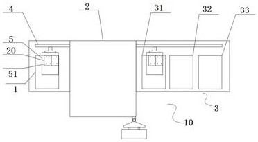
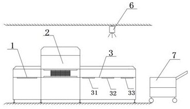
[0037] A method for improving PCB electrical testing efficiency, characterized in that, comprising a testing mechanism 10, comprising the following steps:
[0038] S1. Test preparation, the operator puts the board to be tested into the loading table, and puts two SET or multi-SET circuit boards 20 together according to the direction of the test mold;
[0039] S2. The test is carried out, and the feeding mechanism absorbs two more SET circuit boards and puts them into the test mold;
[0040] The step S2 includes two ways of S21 or S22:
[0041] S21. Multi-SET tests all the PASS, then the controller in the test module sends a signal to all the receiving nozzles, and the receiving mechanism sucks all the SET boards into the PASS area;
[0042] S22. Multi-SET test part PASS, then the controller in the test module sends a signal to the corresponding material receiving nozzle, and the material receiving mechanism sucks the PASS board into the PASS area, and puts the SHORT board or ...
PUM
 Abstract
Description
Claims
Application Information

