Thick film chip winding and planar chip

A winding and chip technology, which is applied in the direction of transformer/inductor coil/winding/connection, electrical components, transformer/inductor parts, etc., can solve the problems of uneven distance between single-chip winding units and increased overall thickness, and achieve increased The effect of making material types and reducing the overall thickness

Inactive Publication Date: 2021-11-26
无锡燊旺和电子科技有限公司
View PDF0 Cites 0 Cited by
  • Summary
  • Abstract
  • Description
  • Claims
  • Application Information

AI Technical Summary

Problems solved by technology

[0004] Aiming at the defects of the prior art, the object of the present invention is to provide a thick-film chip winding and a planar chip, through-holes are processed on each single-chip winding unit, and the single-chip winding units are connected in series and fixed through row pins, thereby maint

Method used


Image

  • Thick film chip winding and planar chip
  • Thick film chip winding and planar chip
  • Thick film chip winding and planar chip

Examples


Embodiment Construction

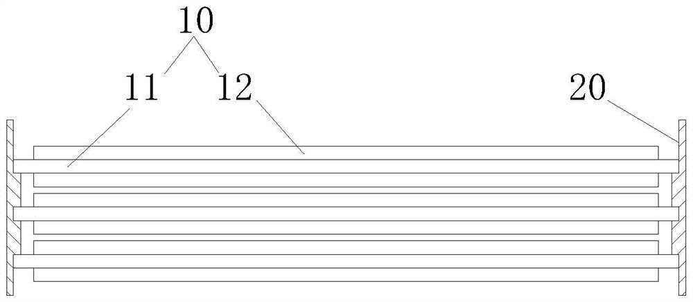
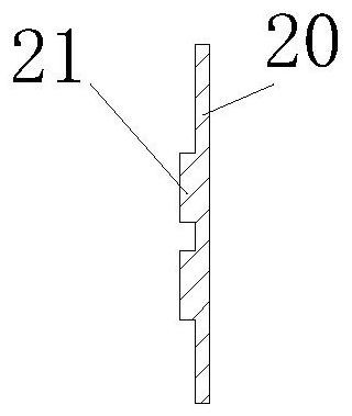
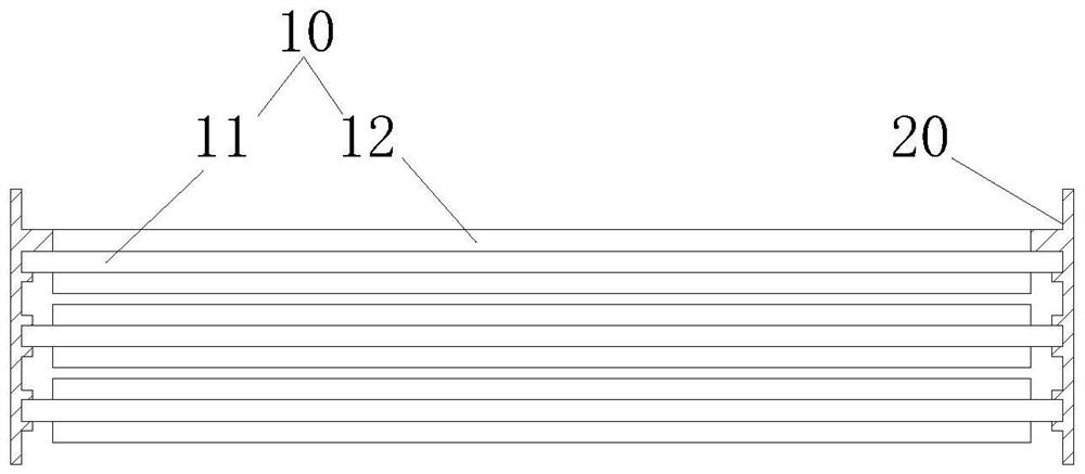
[0039] In order to make the above objects, features and advantages of the present invention more comprehensible, specific implementations of the present invention will be described in detail below in conjunction with the accompanying drawings. In the following description, numerous specific details are set forth in order to provide a thorough understanding of the present invention. However, the present invention can be implemented in many other ways different from those described here, and those skilled in the art can make similar improvements without departing from the connotation of the present invention, so the present invention is not limited by the specific embodiments disclosed below.

[0040] It should be noted that when an element is referred to as being “fixed” to another element, it can be directly on the other element or there can also be an intervening element. When an element is referred to as being "connected to" another element, it can be directly connected to t...


PUM


Abstract

The invention discloses a thick film chip winding and a planar chip. The thick film chip winding comprises more than two single-piece winding units and a plurality of pin headers; each single-piece winding unit comprises an insulating base material and a winding layer, wherein the winding layer is connected to the surface of the insulating base material, and the winding layer comprises at least one winding coil segment; the winding coil segments of more than two single-piece winding units are connected to form at least one winding coil; the side edges of the insulating base materials are fixed by the pin headers, the pin headers connect the more than two single-piece winding units in a series connection mode, a space is reserved between every two adjacent insulating base materials, and the space is determined by the pin headers; and the pin headers are mutually insulated or are conducted through at least one winding coil segment. According to the thick film chip winding provided by the invention, the distance between the two insulating base materials is determined by customizing the pin headers, so that it can be ensured that the distance between the two insulating base materials is equal.

Description

technical field [0001] The invention relates to the technical field of circuit chips, in particular to a thick-film chip winding and a planar chip. Background technique [0002] In the field of chip transformers, commonly used substrates are mainly flexible circuit boards, printed circuit boards, ceramic copper clad laminates, low-temperature co-fired ceramic boards, high-temperature co-fired ceramic boards, etc. Due to the limitation of the process, it is impossible to make a substrate with very thick copper foil for firing ceramic boards. Generally, the copper thickness does not exceed 0.1mm. As the power of the chip transformer gradually increases, and in order to ensure that the volume of the transformer is reduced as much as possible, thicker copper foil is required to make the winding of the chip transformer. At this time, it is more suitable to use printed circuit boards and ceramic copper-clad laminates, but ceramic Copper-clad laminates cannot be multi-layered, so ...

Claims


Application Information

Patent Timeline
IPC IPC(8): H01F27/28H01F27/32
CPCH01F27/2804H01F27/323H01F2027/2809H01F2027/2814H01F2027/2819
Inventor 娄建勇张旭东袁凯姚炜尹玮
Owner 无锡燊旺和电子科技有限公司
Why Eureka
Try Eureka