Developing, film-removing and etching device for high-density circuit board production, and implementation method thereof
A technology for etching devices and circuit boards, which is applied in the removal of conductive materials by chemical/electrolytic methods, and the manufacture of printed circuits and printed circuits. The effect of peeling
- Summary
- Abstract
- Description
- Claims
- Application Information
AI Technical Summary
Problems solved by technology
Method used
Image
Examples
Embodiment 1
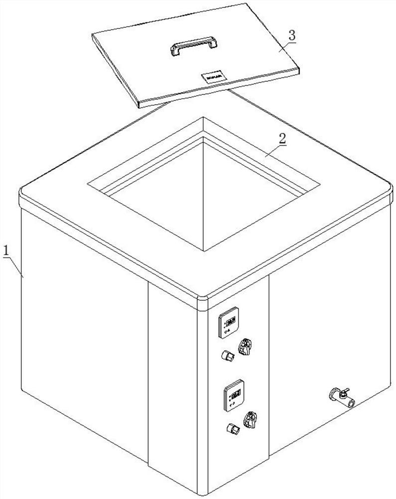
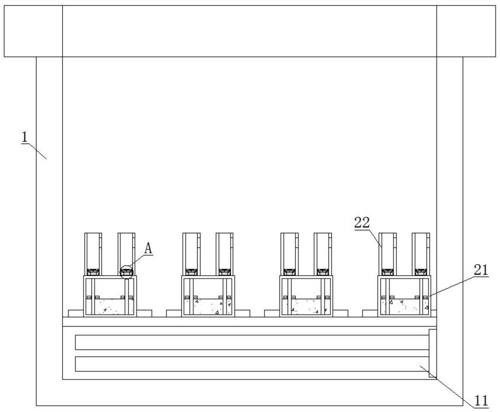
[0034] see Figure 1-2 , the development and film removal etching device for the production of high-density circuit boards, including the etching film removal device 1 and the feeding hole 2 provided at the upper end of the etching film removal device 1, the upper opening of the feeding hole 2 is provided with a first cover plate 3, the etching back film A quartz heating tube 11 is arranged on the bottom surface of the cavity of the membrane device 1 .
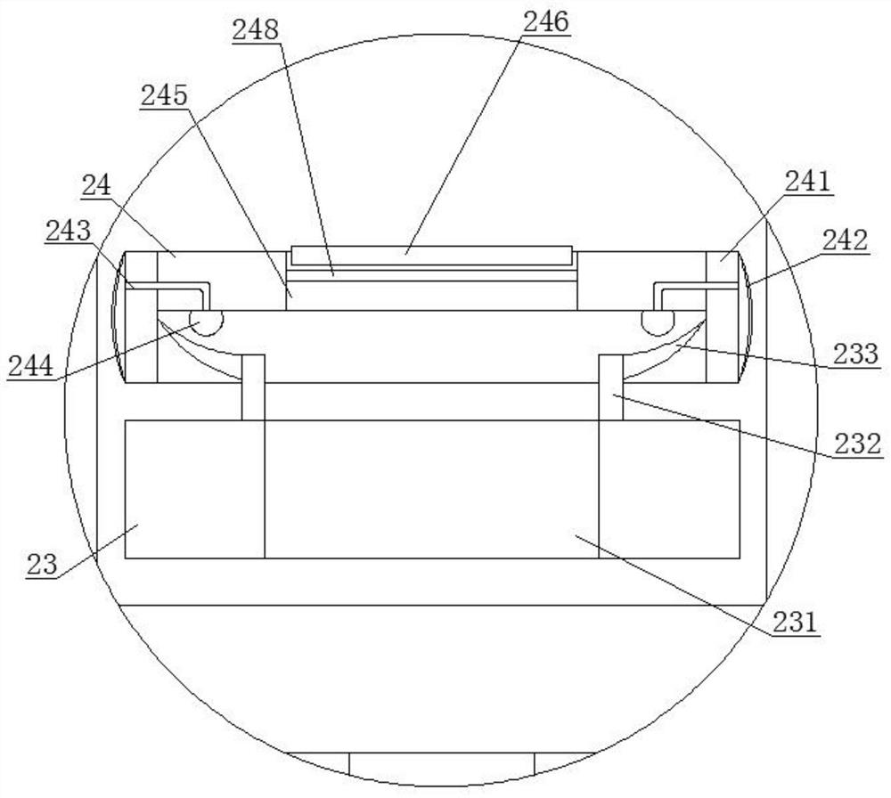
[0035] see Figure 2-4, the bottom surface of the inner cavity of the feed hole 2 is fixedly provided with a low-pressure tank 21, the inner cavity of the low-pressure tank 21 is provided with an aqueous solution 211, and a support rod 212 is provided extending from the bottom surface of the inner cavity of the aqueous solution 211 to the top surface, and the outer surface of the support rod 212 is sleeved with a floating plate 213, the bottom surface of the floating plate 213 is located on the surface of the aqueous solution...
Embodiment 2
[0038] see Figure 1-2 , the development and film removal etching device for the production of high-density circuit boards, including the etching film removal device 1 and the feeding hole 2 provided at the upper end of the etching film removal device 1, the upper opening of the feeding hole 2 is provided with a first cover plate 3, the etching back film A quartz heating tube 11 is arranged on the bottom surface of the cavity of the membrane device 1 .
[0039] see Figure 2-4 , the bottom surface of the inner cavity of the feed hole 2 is fixedly provided with a low-pressure tank 21, the inner cavity of the low-pressure tank 21 is provided with an aqueous solution 211, and a support rod 212 is provided extending from the bottom surface of the inner cavity of the aqueous solution 211 to the top surface, and the outer surface of the support rod 212 is sleeved with a floating plate 213, the bottom surface of the floating plate 213 is located on the surface of the aqueous solutio...
Embodiment approach
[0042] The present invention provides another technical solution: a method for implementing a developing, film-removing and etching device for high-density circuit board production, comprising the following steps:
[0043] S01: The circuit board is placed from the feed hole 2 into the inner cavity of the etching film removal device 1 filled with sodium hydroxide. While the quartz heating tube 11 is heating, the heat is transferred to the inner cavity of the low-pressure tank 21. Because the inner cavity of the low-pressure tank 21 The pressure is low, so that the aqueous solution 211 in the inner cavity of the low-pressure tank 21 can boil and roll quickly;
[0044] S02: While the aqueous solution 211 is boiling and rolling, the floating plate 213 installed on the surface of the aqueous solution 211 undulates up and down together, and the ups and downs of the floating plate 213 make the magnetic force of the first magnetic plate 214 push the second magnetic plate 23 arranged ve...
PUM
 Abstract
Description
Claims
Application Information
 - R&D Engineer
- R&D Manager
- IP Professional
- Industry Leading Data Capabilities
- Powerful AI technology
- Patent DNA Extraction
Browse by: Latest US Patents, China's latest patents, Technical Efficacy Thesaurus, Application Domain, Technology Topic, Popular Technical Reports.
© 2024 PatSnap. All rights reserved.Legal|Privacy policy|Modern Slavery Act Transparency Statement|Sitemap|About US| Contact US: help@patsnap.com


