Glitch-free multiplexer and glitch transmission prevention

A circuit and decoder technology, applied in the direction of pulse technology, pulse processing, electrical components, etc.

Pending Publication Date: 2022-01-04
NVIDIA CORP
View PDF0 Cites 0 Cited by
  • Summary
  • Abstract
  • Description
  • Claims
  • Application Information

AI Technical Summary

Problems solved by technology

However, multiple paths through combinatorial logic can cause the signal outpu...

Method used


Image

  • Glitch-free multiplexer and glitch transmission prevention
  • Glitch-free multiplexer and glitch transmission prevention
  • Glitch-free multiplexer and glitch transmission prevention

Examples


Embodiment Construction

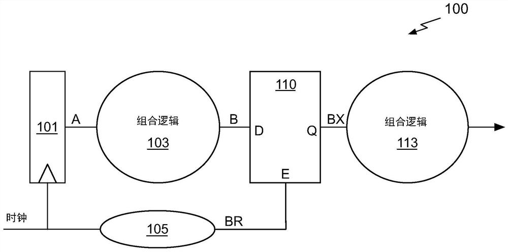
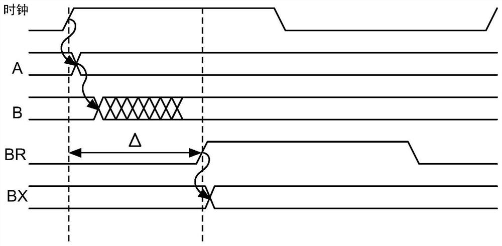
[0029] In response to the changed data and selection input, the output of the multi-transistor can change multiple times before stabilizing to the final state. In the context described below, the change is a transition of the voltage level that identifies it as a different state. For example, the change is identified as an assigned state compared to the reverse or not assigned state. In another example, the change is a transition from a high level to a low level or from a low level to a high level. In the context described below, a stable or constant level can vary while the range of voltage values ​​identified as the same state (eg, logic is true or logic is fake).

[0030] Multiple changes in the output of the multiplexers are considered to be burrs, and the combined logic of the received output can respond by charging and / or discharging and dissipating power by charging and / or discharging and dissipating power by charging and / or discharging and dissipating power by chargi...


PUM


Abstract

When a signal glitches, logic receiving the signal may change in response, thereby charging and/or discharging nodes within the logic and dissipating power. Providing a glitch-free signal may reduce the number of times the nodes are charged and/or discharged, thereby reducing the power dissipation. A technique for eliminating glitches in a signal is to insert a storage element that samples the signal after it is done changing to produce a glitch-free output signal. The storage element is enabled by a 'ready' signal having a delay that matches the delay of circuitry generating the signal. The technique prevents the output signal from changing until the final value of the signal is achieved. The output signal changes only once, typically reducing the number of times nodes in the logic receiving the signal are charged and/or discharged so that power dissipation is also reduced.

Description

Technical field [0001] The present disclosure relates to preventing glitch (GLITCH) from propagating in the circuit. In particular, the present disclosure relates to eliminate burrs in the signal by inserting a storage element that sampling signal samples to generate a burning output signal. Background technique [0002] The conventional sequence circuit includes a combined logic having an input by a synchronization register or trigger. "Combined Logic" refers to a logic that receives one or more inputs, combines these inputs to generate output, without storing the state of input, output, or any intermediate value. In other words, the combined logic is "stateless" and can be asynchronous (not being driven by the clock signal). In contrast, for the sequence circuit (logic), the register is stored. [0003] At the rising edge of the clock, the output of the register is just changing once. However, multiple paths of combined logic may cause multiple changes to occur before the signa...

Claims


Application Information

Patent Timeline
IPC IPC(8): H03K5/1252H03K5/01
CPCH03K5/1252H03K5/01
Inventor W·J·达利
Owner NVIDIA CORP
Why Eureka
Try Eureka