Unlock instant, AI-driven research and patent intelligence for your innovation.

Wafer pre-alignment device and pre-alignment method

An alignment device and pre-alignment technology, applied in the direction of electrical components, semiconductor/solid-state device manufacturing, circuits, etc., can solve problems such as inability to identify

Pending Publication Date: 2022-01-11
SHANGHAI GUONA SEMICON TECH CO LTD
View PDF1 Cites 8 Cited by
  • Summary
  • Abstract
  • Description
  • Claims
  • Application Information

AI Technical Summary

Problems solved by technology

[0004] In order to overcome the above-mentioned shortcomings, the object of the present invention is to provide a wafer pre-alignment device, which can reduce the problem of abnormalities that cannot be detected by the original visual inspection unit due to excessive wafer offset, shorten downtime, and improve equipment Overall stability, reducing the risk of excessive wafer offset and unrecognizable risks; to a certain extent, it can improve the compensation range of the pre-alignment device

Method used


Image

  • Wafer pre-alignment device and pre-alignment method
  • Wafer pre-alignment device and pre-alignment method
  • Wafer pre-alignment device and pre-alignment method

Examples


Embodiment 1

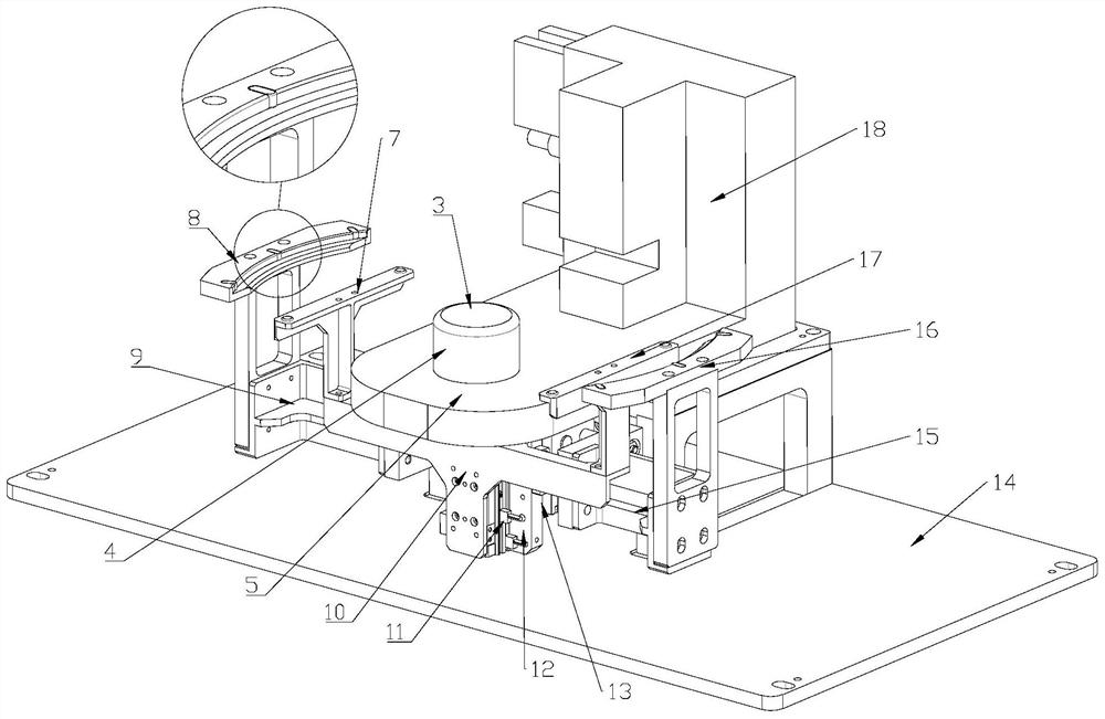
[0029] See attached Figure 1-2 As shown, a wafer 6 pre-alignment device of the present invention includes a bottom plate 14, above which is provided a carrying plate 5 parallel to it, and the carrying plate 5 is fixed on the bottom plate 14 through a fixing frame. The carrying plate 5 is provided with a rotating base 4, and the rotating base 4 is provided with a vacuum adsorption platform 3 which rotates synchronously with it. The vacuum adsorption platform 3 can absorb the wafer 6, and the rotating base 4 drives the vacuum adsorption platform 3 and the wafer 6 to synchronize. turn. One side of the rotating base 4 is provided with a visual inspection unit 18 for precise alignment of the wafer 6. The visual inspection unit 18 includes a stand fixed on one side of the rotating base 4, and a CCD vision sensor and a backlight are arranged on the stand. The vacuum adsorption platform 3 adsorbs and fixes the wafer 6, the rotating base 4 drives the wafer 6 on the vacuum adsorption ...

Embodiment 2

[0042] Refer to attached Figure 5-6 As shown, the difference between this embodiment and Embodiment 1 is only the difference in the jacking device. In this embodiment, the jacking device includes a jacking drive member 11 and a mounting seat 20. The mounting seat 20 is fixed on the bottom plate 14, and the jacking drive The output shaft of the part 11 is fixedly connected with the centering drive part, and the jacking drive part 11 drives the centering device to go up and down. The lifting driver 11 directly drives the centering device up and down, and the wafer 6 is lifted up by the groove bottoms of the left centering baffle 8 and the right centering baffle 16 of the centering device, and then centered. Other structures are the same as in Example 1.

[0043] The jacking device of this embodiment directly lifts up the centering device, so that the left centering baffle 8 and the right centering baffle 16 of the centering device can lift the wafer 6 on the vacuum adsorption ...


PUM


Abstract

The invention discloses a wafer pre-alignment device, and the device comprises a bottom plate; a bearing plate parallel to the bottom plate is arranged above the bottom plate, a rotating base is arranged on the bearing plate, a vacuum adsorption platform rotating synchronously with the rotating base is arranged on the rotating base, and a visual detection unit used for accurately aligning a wafer is arranged on one side of the rotating base. The device also comprises a jacking centering mechanism which is arranged on the bottom plate, can jack up or put down the wafer on the vacuum adsorption platform, and can push the wafer to horizontally move relative to the vacuum adsorption platform until the circle center of the wafer coincides with the center line of the vacuum adsorption platform. The invention further discloses an alignment method based on the device, the jacking and centering mechanism is additionally arranged, the problem that due to the fact that the deviation of the wafer is too large, an original visual detection unit cannot detect abnormity is solved, the downtime is shortened, the overall stability of equipment is improved, and the risk that the deviation of the wafer is too large and cannot be recognized is reduced; and the compensation range of the pre-alignment device can be improved to a certain extent.

Description

technical field [0001] The invention relates to the technical field of wafer processing equipment, in particular to a wafer pre-alignment device and a pre-alignment method. Background technique [0002] The positioning and identification of the wafer is an important link in the wafer handling and the entire IC manufacturing process. The positioning and identification of the wafer require the reference of the pre-aligner (Pre-Aligner). The purpose of wafer pre-alignment is to calculate the eccentricity of the wafer and find its notch, and then compensate for its eccentricity and turn the notch to a certain direction to prepare for the next step of wafer identification and processing. Existing wafer pre-alignment device refers to attached Figure 7-8 As shown, it includes a rotating base 4' fixed on a carrier plate 5', a vacuum adsorption platform 3' is fixed on the rotating base 4', a CCD vision sensor 1' is provided on one side of the rotating base 4' through a stand, and a ...

Claims


Application Information

Patent Timeline
IPC IPC(8): H01L21/68
CPCH01L21/68H01L21/681
Inventor 章秀国叶莹
Owner SHANGHAI GUONA SEMICON TECH CO LTD
Features
  • R&D
  • Intellectual Property
  • Life Sciences
  • Materials
  • Tech Scout
  • Unparalleled Data Quality
  • Higher Quality Content
  • 60% Fewer Hallucinations
Learn More