Pixel driving circuit and display panel

a driving circuit and display panel technology, applied in the field of display technology, can solve the problems of affecting material stability and lifespan of the display, unable to fully detect the threshold voltage, and unable to further compensate the threshold voltage vth

Active Publication Date: 2022-09-27
SHENZHEN CHINA STAR OPTOELECTRONICS SEMICON DISPLAY TECH CO LTD
View PDF15 Cites 0 Cited by
  • Summary
  • Abstract
  • Description
  • Claims
  • Application Information

AI Technical Summary

Benefits of technology

[0007]The present disclosure provides a pixel driving circuit and a display panel, which combine a gate regulation principle of doubled-gate devices and a threshold voltage detection principle of diode structures to realize compensation for a threshold voltage of driving thin film transistors being positive and negative, so that a problem that traditional diode-connect type internal compensation circuit can only compensate for a threshold voltage drift in a single direction is solved, thereby improving accuracy and uniformity of images displayed.
[0031]Compared with the prior art, in the pixel driving circuit provided by the present disclosure, the driving thin film transistor in the compensation driving module adopts a doubled-gate structure. According to the gate regulation principle of doubled-gate devices, a potential of the bottom gate of the doubled-gate driving thin film transistor can linearly dynamically adjust the threshold voltage. In the initial stage, the bottom gate of the doubled-gate driving thin film transistor is charged to a high potential, and the threshold voltage is adjusted to a lower initial value. Then, combined the threshold voltage detection principle of diode structures, in the threshold voltage compensation stage, the bottom gate and the drain of the doubled-gate driving thin film transistor are short-circuited to form a diode structure, thereby gradually decreasing a high potential of the bottom gate until the doubled-gate driving thin film transistor is turned off, so that the threshold voltage is equal to the voltage difference between the top gate and the source of the doubled-gate driving thin film transistor. Since the potential of the top gate is equal to the reference voltage and the potential of the source is equal to the second power source voltage in this stage, the threshold voltage after compensation is equal to a difference between the reference voltage and the second power source voltage in the compensation stage, thereby realizing a compensation of the threshold voltage of the doubled-gate driving thin film transistor. In addition, regardless of whether the threshold voltage of the doubled-gate driving thin film transistor is positive or negative before initialization, the threshold voltage of the doubled-gate driving thin film transistor can be adjusted to the initial value by increasing the potential of the bottom gate of the doubled-gate driving thin film transistor and then compensate thereof. Therefore, the pixel driving circuit of the present disclosure can realize the compensation for the threshold voltage being positive and negative, effectively broadening a compensation range of the threshold voltage, which solves the problem that traditional diode-connect type internal compensation circuit can only compensate for the threshold voltage drift in a single direction, and is beneficial to improve display accuracy and display uniformity of the display panels and lifespan of the display panels.

Problems solved by technology

However, OLEDs are organic materials which are sensitive to water, oxygen, etc., affecting material stability and lifespan of the displays.
Thus, the gate (G) cannot fully detect the threshold voltage Vth information and cannot further compensate the threshold voltage Vth.
Therefore, for N-type thin film transistors, the traditional diode-connect type compensation circuit cannot compensate for a negative Vth, which is inconducive to improving display uniformity of panels, and reduces the lifespan of the panels.

Method used


Image

  • Pixel driving circuit and display panel
  • Pixel driving circuit and display panel
  • Pixel driving circuit and display panel

Examples


Embodiment Construction

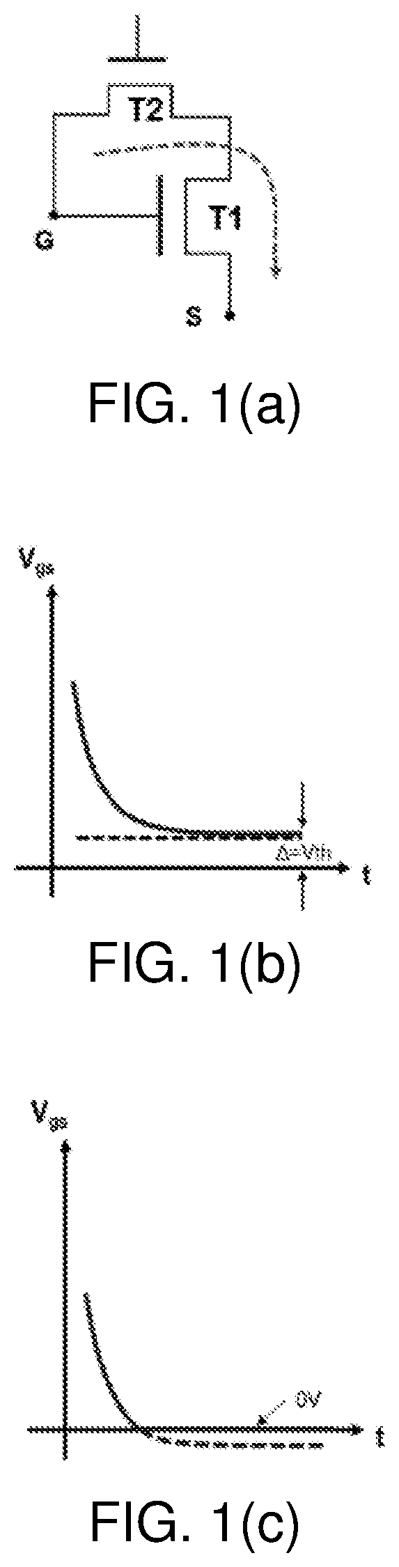
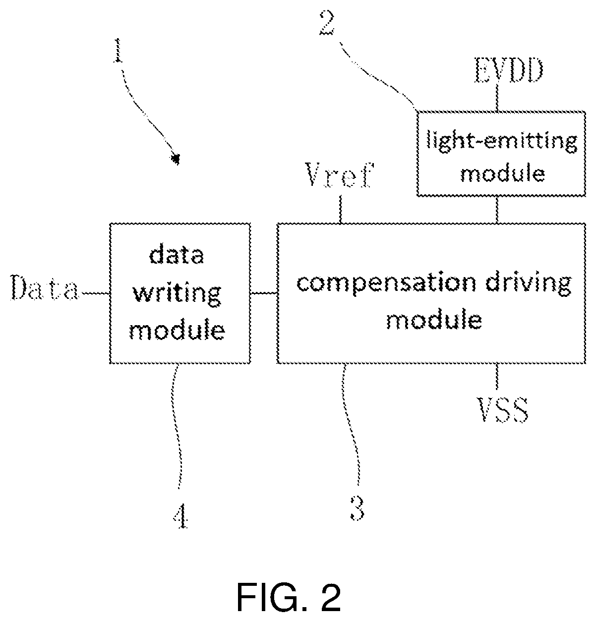
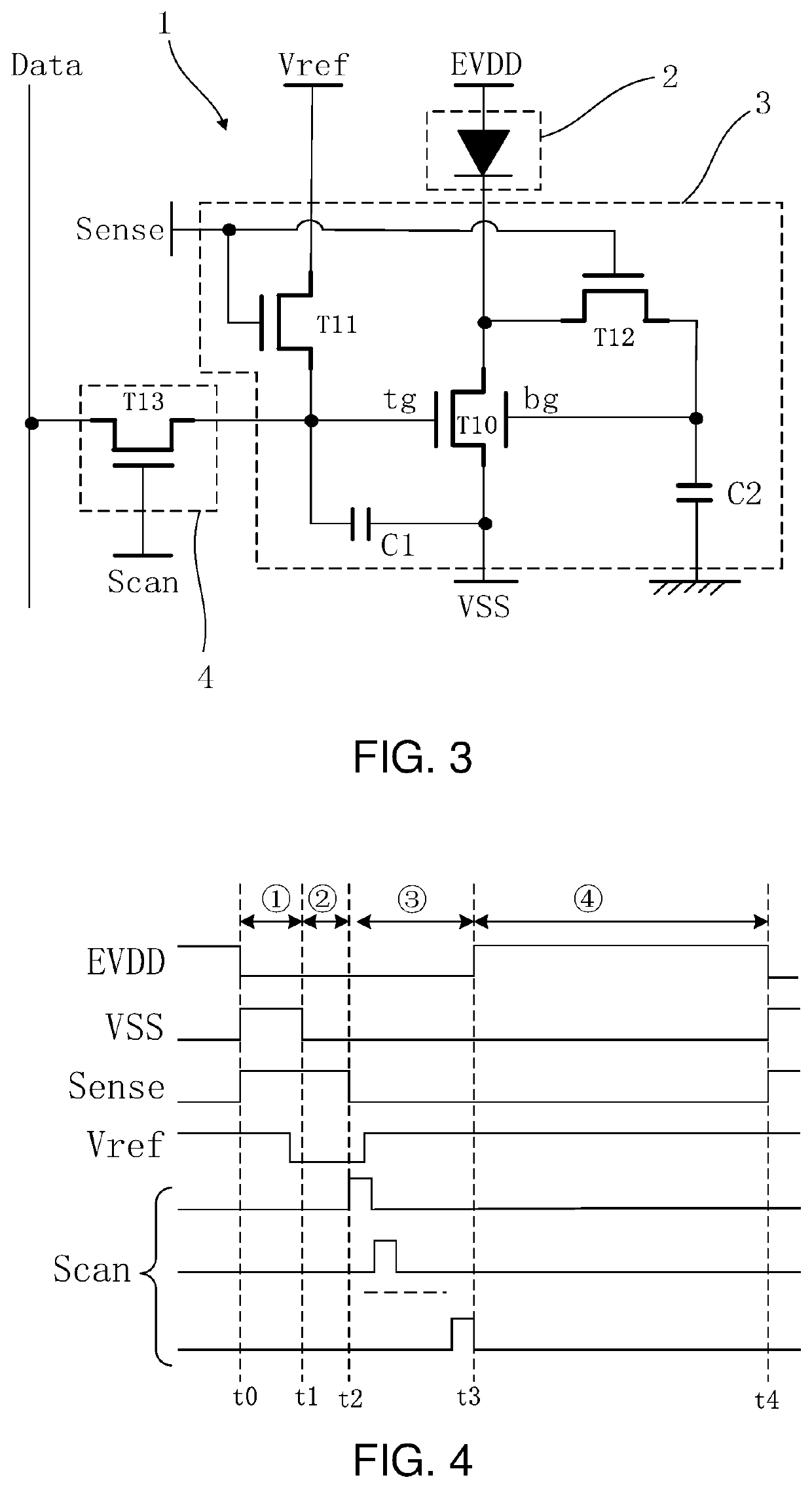
[0042]The technical solutions in the embodiments of the present disclosure will be clearly and completely described below in conjunction with accompanying drawings in the embodiments of the present disclosure. Obviously, the embodiments described are merely a part of the present disclosure, rather than all the embodiments. All other embodiments obtained by the person having ordinary skill in the art based on embodiments of the disclosure, without making creative efforts, are within the scope of the present disclosure.

[0043]The following disclosure provides many different embodiments or examples for achieving different structures of the present disclosure. To simplify the present disclosure, components and settings of specific examples are described below. They are only examples and are not intended to limit the present disclosure. In addition, the present disclosure may repeat reference numbers and / or reference letters in different examples, this repetition is for the purpose of sim...


PUM

PropertyMeasurementUnit
threshold voltage Vthaaaaaaaaaa
threshold voltageaaaaaaaaaa

Abstract

The present invention provides a pixel driving circuit and a display panel. The pixel driving circuit includes a light emitting module and a compensation driving module which are electrically connected. The compensation driving module includes a doubled-gate driving thin film transistor, and is configured to charge a bottom gate of the doubled-gate driving thin film transistor and adjust a threshold voltage to an initial value in an initial stage. The compensation driving module receives a reference voltage to discharge the bottom gate of the doubled-gate driving thin film transistor in a threshold voltage compensation, realizing a compensation of the threshold voltage.

Description

RELATED APPLICATIONS[0001]This application is a Notional Phase of PCT Patent Application No. PCT / CN2020 / 087697 having international filing date of Apr. 29, 2020, which claims the benefit of priority of Chinese Patent Application No. 202010274095.1 filed on Apr. 9, 2020. The contents of the above applications are all incorporated by reference as if fully set forth herein in their entirety.FIELD OF INVENTION[0002]The present disclosure relates to the field of display technology, and more particularly, to a pixel driving circuit and a display panel.BACKGROUND OF INVENTION[0003]Compared with liquid crystal display (LCD) technology, organic light-emitting diode (OLED) displays have advantages of higher contrast, faster response speed, and wide viewing angle, and are widely applied in a field of smart phones, smart TVs, and wearable devices. However, OLEDs are organic materials which are sensitive to water, oxygen, etc., affecting material stability and lifespan of the displays. In recent...

Claims


Application Information

Patent Timeline
Patent Type & Authority Patents(United States)
IPC IPC(8): G09G3/3291G09G3/3233G09G3/3258G09G3/3266
CPCG09G3/3291G09G3/3233G09G3/3258G09G3/3266G09G3/32G09G3/3208G09G2320/0233G09G2320/045G09G2300/0866G09G2300/0426G09G2310/08G09G2320/043G09G2300/0861
Inventor ZHANG, XIAODONGSONG, SANGCHEOL
Owner SHENZHEN CHINA STAR OPTOELECTRONICS SEMICON DISPLAY TECH CO LTD
Why Eureka
Try Eureka