Superconducting digital circuit structure capable of inhibiting quasi-particle poisoning and manufacturing method thereof
A technology of digital circuits and manufacturing methods, applied in the field of superconducting quantum, can solve the problems of quasi-particle poisoning of superconducting digital circuits, and achieve the effect of reducing loss
- Summary
- Abstract
- Description
- Claims
- Application Information
AI Technical Summary
Problems solved by technology
Method used
Image
Examples
Embodiment 1
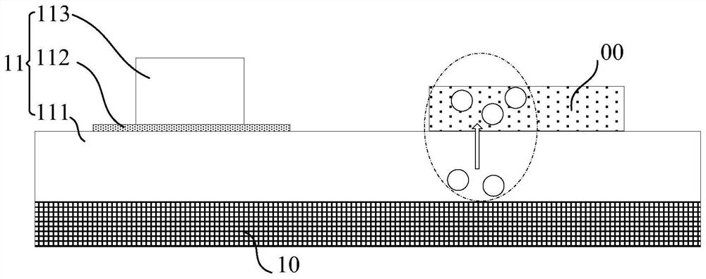
[0054] The superconducting digital circuit structure capable of suppressing quasiparticle poisoning of the present invention includes a substrate, a superconducting structure and a normal metal layer; the superconducting structure is arranged on the substrate 10, and the normal metal layer is electrically connected to the superconducting The bottom electrode 111 of the conductive structure, and the normal metal layer 00 is used to suppress the quasi-particles generated by the superconducting digital circuit.
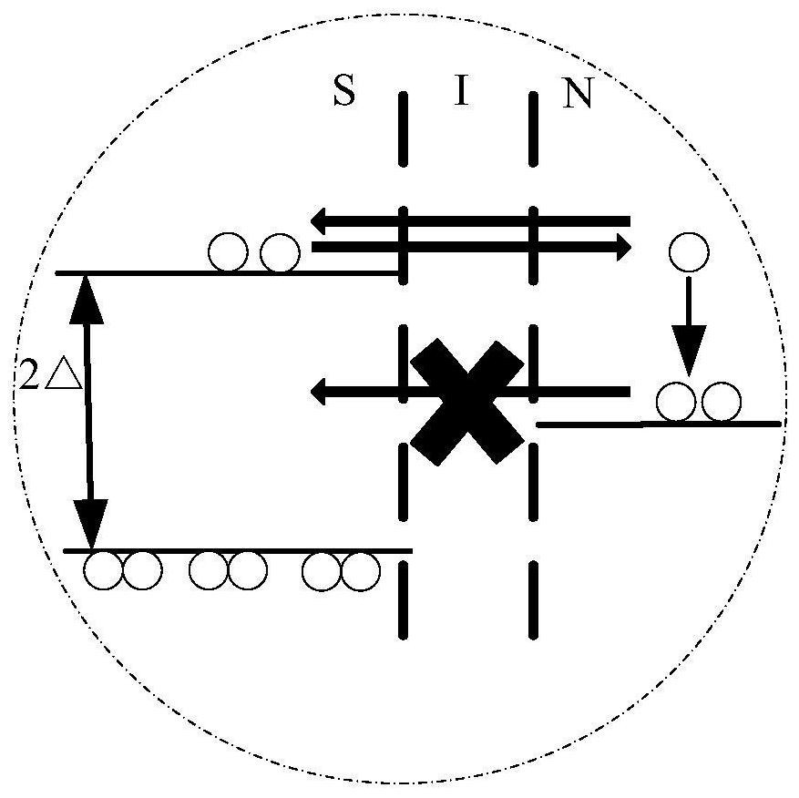
[0055] Based on the above principles, the present invention proposes a superconducting digital circuit structure that can suppress quasiparticle poisoning. The superconducting digital circuit structure manufactures normal metal traps that can suppress quasiparticle poisoning through normal metal layers, which can reduce and reduce the generation of quasiparticles to achieve the effect of suppressing quasiparticle poisoning.
[0056] The superconducting structure of the p...
Embodiment 2
[0082] In order to solve the above-mentioned technical problems, the present invention also provides a method for manufacturing a superconducting digital circuit structure that can suppress quasiparticle poisoning, and the method for manufacturing at least includes the following steps:
[0083] S1, providing the substrate,
[0084] The substrate in this embodiment serves as the structural basis of the entire superconducting digital circuit structure;
[0085] S2, sequentially forming three layers of films on the surface of the substrate, and etching the three layers of films to form a Josephson junction, the Josephson junction includes a bottom electrode, a first insulating material layer and a top electrode; the first insulating material layer is set between the bottom electrode and the top electrode; the bottom electrode is disposed on the substrate;
[0086] The three-layer film in this step is the bottom electrode (L1 layer), the first insulating material layer (L2 layer)...
PUM
| Property | Measurement | Unit |
|---|---|---|
| Thickness | aaaaa | aaaaa |
| Thickness | aaaaa | aaaaa |
| Thickness | aaaaa | aaaaa |
Abstract
Description
Claims
Application Information


