Packaging structure and packaging method of high-power radio frequency device

A technology of radio frequency device and packaging structure, which is applied in the manufacturing of semiconductor devices, electric solid state devices, and semiconductor/solid state devices, etc., can solve the problem of inability to achieve high power output, save product development cycle, realize mass production, and improve utilization rate Effect

Pending Publication Date: 2022-01-25
INNOGRATION SUZHOU
View PDF0 Cites 2 Cited by
  • Summary
  • Abstract
  • Description
  • Claims
  • Application Information

AI Technical Summary

Problems solved by technology

At present, the internal chip layout structure of mainstream high-power RF power amplifier devices is as follows: figure 1 shown, combined with figure 2 As shown, multiple chips 1 are assembled in parallel inside the same package 4, the chip 1 is parallel to the package cavity 5, multiple chips 1 are welded side by side on the package flange 6, and the lead wire (Bond-wire) direction of the chip 1 is in line with the chip welding The direction of the plate (BondPad) is vertical, and the other ends of the input lead 3 and the output lead 2 are soldered to pin 7. The input lead 3 and the output lead 2 will not cross over the chip 1, and there will be no space between the input lead 3 and the output lead 2. However, limited by the size of the chip and the size of the internal cavity of the package, it is impossible to achieve the purpose of higher power output

Method used


Image

  • Packaging structure and packaging method of high-power radio frequency device
  • Packaging structure and packaging method of high-power radio frequency device
  • Packaging structure and packaging method of high-power radio frequency device

Examples


Embodiment

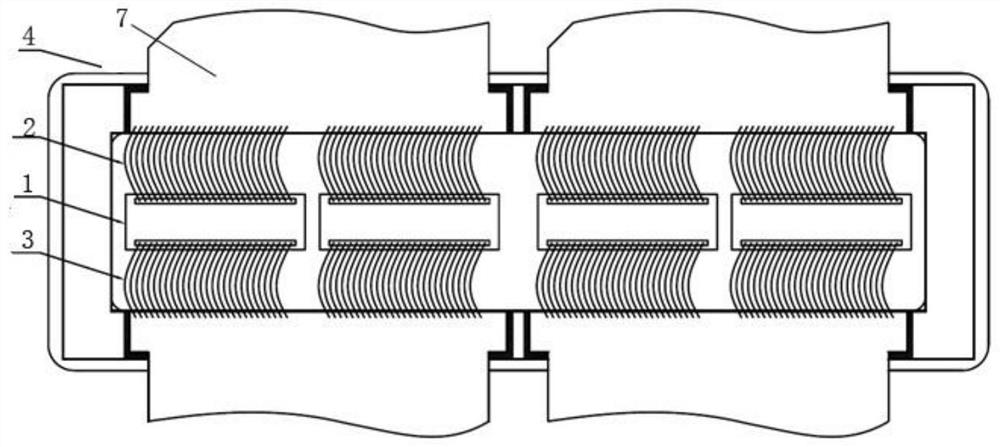
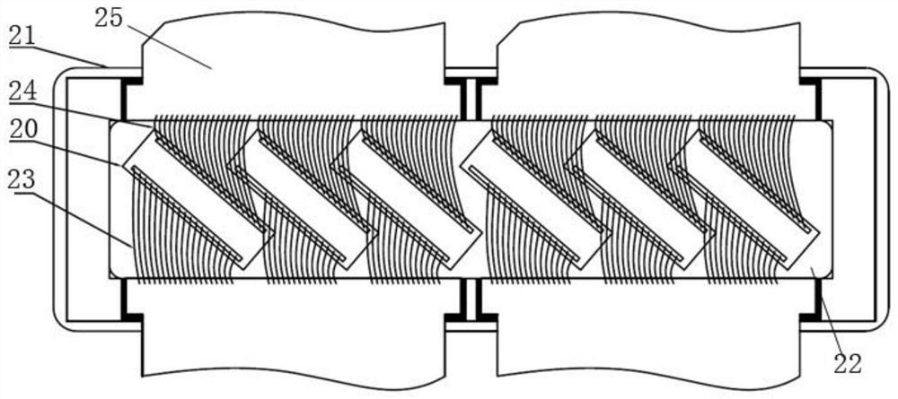
[0030] Such as image 3 , 4 As shown, the packaging structure of the high-power radio frequency device of the present invention includes a plurality of parallel radio frequency power chips 20 and a packaging flange 21, and a plurality of radio frequency power chips 20 are obliquely arranged in the packaging cavity 22 of the packaging flange 21, and many Each RF power chip 20 forms a certain angle with the package cavity 22, and multiple RF power chips 20 are preferably arranged in parallel at the same angle. The subsequent process can be made simpler. The number of RF power chips depends on the selected package size and the selected chip size.

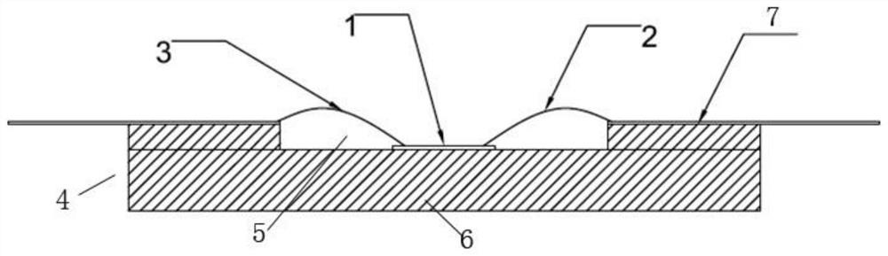
[0031] Such as Figure 5 As shown, when the inclination angle ∠A is determined, the distance between the outermost end of the radio frequency power chip 20 and the package cavity 22 is greater than or equal to a set threshold, such as the minimum distance d. Specifically, the maximum inclination angle cannot make the distance betwe...


PUM


Abstract

The invention discloses a packaging structure of a high-power radio frequency device, which comprises a plurality of radio frequency power chips connected in parallel and a packaging flange. The plurality of radio frequency power chips are obliquely arranged in a packaging inner cavity of the packaging flange, so that the number of input leads of the radio frequency power chips is reduced, and the input leads and output leads are not overlapped in space. The plurality of chips are obliquely arranged on the packaging flange, so that the utilization rate of the packaging space is remarkably improved, and the purpose of higher power output is achieved. By slightly reducing the number of the input leads of the intermediate radio-frequency power chip, the output leads cannot be reduced, the reliability of a high-power application process can be ensured, large-area overlapping of the input leads and the output leads in space is avoided, mutual inductance is reduced, and oscillation of the radio-frequency power device is effectively avoided.

Description

technical field [0001] The invention relates to the technical field of packaging of radio frequency devices, in particular to a packaging structure and a packaging method of high-power radio frequency devices. Background technique [0002] Mainstream RF power chips usually consider factors such as product performance and heat dissipation, and the size of the chip is mostly rectangular with a large aspect ratio. Limited by the production and assembly process, a single chip will not be made very large. When the output power of a single chip cannot meet the requirements, most of them are assembled in the same package by using multiple chips in parallel. At present, the internal chip layout structure of mainstream high-power RF power amplifier devices is as follows: figure 1 shown, combined with figure 2 As shown, multiple chips 1 are assembled in parallel inside the same package 4, the chip 1 is parallel to the package cavity 5, multiple chips 1 are welded side by side on th...

Claims


Application Information

Patent Timeline
Patent Type & Authority Applications(China)
IPC IPC(8): H01L25/18H01L21/56H01L23/31H01L23/495
CPCH01L25/18H01L23/3121H01L23/49575H01L21/56H01L23/4951H01L23/31H01L23/495H01L23/48H01L21/50H01L2224/49111H01L2224/48091H01L2223/6611H01L24/85H01L2924/00014H01L23/66H01L24/48H01L24/49H01L25/072H01L2224/48011H01L2224/48157H01L2224/4911
Inventor 卓英浩肖智敏竹磊
Owner INNOGRATION SUZHOU
Why Eureka
Try Eureka