Supercharge Your Innovation With Domain-Expert AI Agents!

Memory device and method of forming the same

A storage element, charge storage technology, applied in electrical components, electrical solid state devices, semiconductor devices, etc.

Pending Publication Date: 2022-01-25
MACRONIX INT CO LTD
View PDF0 Cites 0 Cited by
  • Summary
  • Abstract
  • Description
  • Claims
  • Application Information

AI Technical Summary

Problems solved by technology

However, 3D memory elements with vertical channel structures still face many challenges

Method used


Image

  • Memory device and method of forming the same
  • Memory device and method of forming the same
  • Memory device and method of forming the same

Examples


Embodiment Construction

[0065] In order to make the object, technical solution and advantages of the present invention clearer, the present invention will be described in further detail below in conjunction with specific embodiments and with reference to the accompanying drawings.

[0066] However, the present invention can be implemented in various forms, and is not limited to the embodiments described herein. In the drawings, the thicknesses of layers and regions may be exaggerated for clarity. The same or similar component symbols represent the same or similar components, and the following paragraphs will not repeat them one by one.

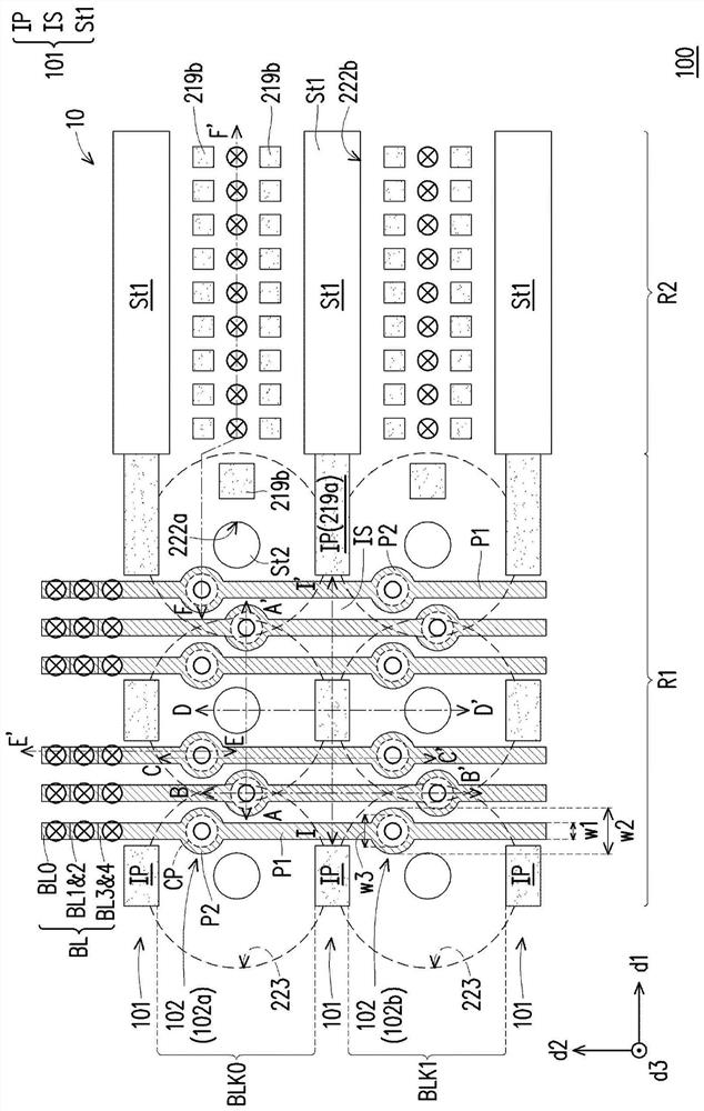
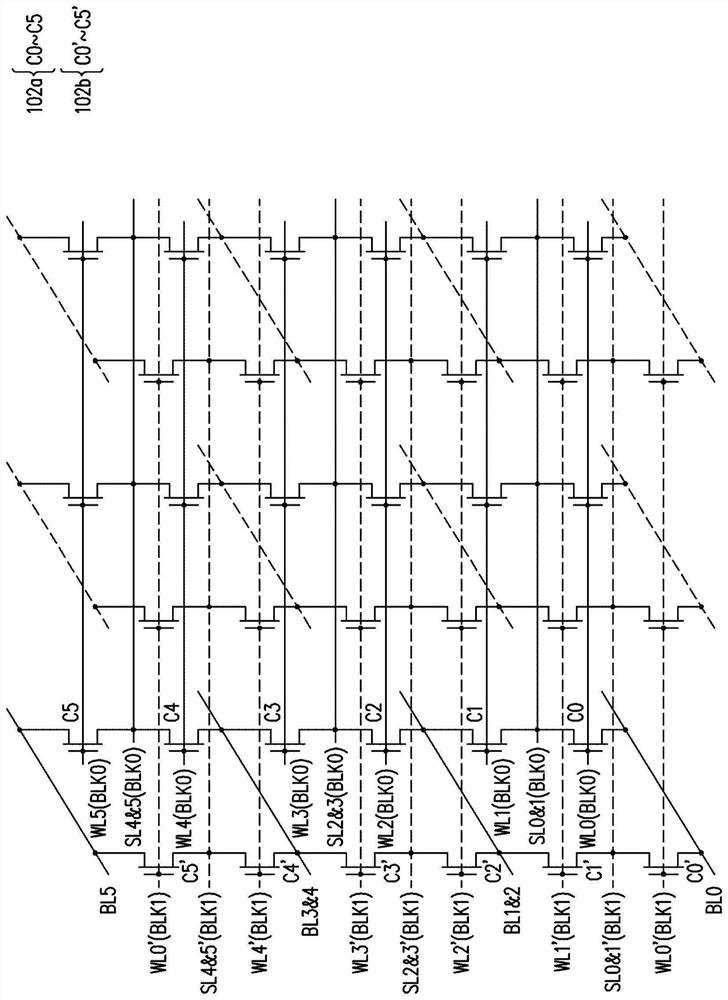
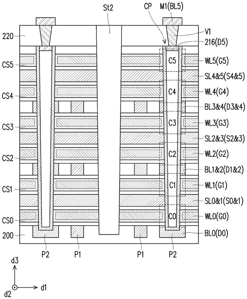
[0067] figure 1 A plan view of a memory element according to some embodiments of the invention is shown. figure 2 shows that according to some embodiments of the present invention figure 1 The local equivalent circuit diagram of the storage element. Figure 3A , Figure 3B , Figure 3C , Figure 3D , Figure 3E , Figure 3F respectively show the edges of so...


PUM


Abstract

A memory device and method of forming the same are provided. The memory device includes a word line, a bit line, a source line, a channel pillar, and a charge storage structure. The bit line and the source line are disposed on opposite sides of the word line in a vertical direction. The channel pillar penetrates through and is connected to the word line, the bit line and the source line. The charge storage structure surrounds a top surface and a bottom surface of the word line and is laterally sandwiched between the channel pillar and the word line. The channel pillar completely penetrates through and is laterally surrounded by the bit line.

Description

technical field [0001] The present invention relates to a memory element and its manufacturing method. Background technique [0002] As technology advances with each passing day, advances in electronic components have increased the need for greater storage capacity. In order to meet the requirement of high storage density, the size of memory elements becomes smaller and higher in density. Therefore, the type of memory device has been developed from a 2D memory device with a planar gate structure to a 3D memory device with a vertical channel (VC) structure. However, 3D memory elements with vertical channel structures still face many challenges. Contents of the invention [0003] Embodiments of the present invention provide a memory element and a manufacturing method thereof. The method can increase the number of vertically stacked memory cells formed in a unit area, so as to effectively use the area of ​​the substrate and increase the density of the memory cells. [0004...

Claims


Application Information

Patent Timeline
Patent Type & Authority Applications(China)
IPC IPC(8): H01L27/11521H01L27/11556H01L27/11568H01L27/11582H10B41/30H10B43/27H10B41/27H10B43/30H10B43/35H10B43/40
CPCH10B41/30H10B41/27H10B43/30H10B43/27H10B43/10H01L23/5226H10B43/35H10B43/40
Inventor 李智雄
Owner MACRONIX INT CO LTD
Features
  • R&D
  • Intellectual Property
  • Life Sciences
  • Materials
  • Tech Scout
  • Unparalleled Data Quality
  • Higher Quality Content
  • 60% Fewer Hallucinations
Learn More