Supercharge Your Innovation With Domain-Expert AI Agents!

Embedded circuit board and manufacturing method thereof

A manufacturing method and circuit board technology, which are applied in multilayer circuit manufacturing, printed circuit manufacturing, printed circuit and other directions, can solve problems such as large loss of raw materials, and achieve the effect of easy miniaturization and realization of miniaturization

Pending Publication Date: 2022-01-25
QING DING PRECISION ELECTRONICS HUAIAN CO LTD +1
View PDF0 Cites 0 Cited by
  • Summary
  • Abstract
  • Description
  • Claims
  • Application Information

AI Technical Summary

Problems solved by technology

In this method, the metal layer arranged on the surface of the substrate is usually the whole surface, but the resistive material layer that finally forms the resistance only occupies a small part of it, resulting in a large loss of raw materials
Moreover, in this manufacturing process, the resistive material layer is stacked with the conductive material layer for making the wiring during the prefabrication process, which will have a negative impact on the transmission loss of the wiring due to material and process problems; and, the manufacturing tolerance of the resistor is often determined by The accuracy of the etching process is determined

Method used


Image

  • Embedded circuit board and manufacturing method thereof
  • Embedded circuit board and manufacturing method thereof
  • Embedded circuit board and manufacturing method thereof

Examples


Embodiment Construction

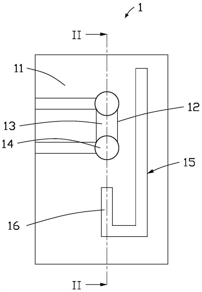
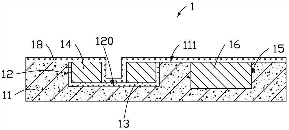
[0067] The following description will refer to the accompanying drawings in order to describe the present disclosure more fully. Exemplary embodiments of the invention are shown in the drawings. This invention may, however, be embodied in many different forms and should not be construed as limited to the exemplary embodiments set forth herein. Rather, these exemplary embodiments are provided so that this disclosure will be thorough and complete, and will fully convey the scope of the invention to those skilled in the art. Like reference numerals designate the same or similar components.

[0068] The terminology used herein is for the purpose of describing particular exemplary embodiments only and is not intended to be limiting of the invention. As used herein, the singular forms "a", "an" and "the" are intended to include the plural forms as well, unless the context clearly dictates otherwise. Furthermore, when used herein, "comprises" and / or "comprises" or "includes" and / o...


PUM

PropertyMeasurementUnit
Thicknessaaaaaaaaaa

Abstract

The invention provides a method for manufacturing an embedded circuit board, and the method comprises the following steps: providing a first base material which comprises a first surface, forming a hole groove in the first surface, and taking the exposed surface of the hole groove as a second surface; forming a resistance material layer on one side of the first base material where the hole groove is formed, reserving the resistance material layer on the second surface to form an embedded resistor, and removing the resistance material layer which is not arranged on the second surface; forming a mask on the side, wherein the hole groove is formed, of the first base material, the mask comprises a first sub-mask, and the first sub-mask is arranged in the hole groove and divides the hole groove into a first sub-groove and a second sub-groove which are spaced; and forming a conductive pin in each of the first sub-slot and the second sub-slot. The invention also provides an embedded circuit board.

Description

technical field [0001] The invention relates to the technical field of embedded circuit boards, in particular to an embedded circuit board and a manufacturing method thereof. Background technique [0002] In recent years, electronic products are widely used in daily work and life, and light, thin and small electronic products are becoming more and more popular. As the main component of electronic products, circuit boards occupy a large space of electronic products. Therefore, the volume of circuit boards affects the volume of electronic products to a large extent. Short and small trends. Among them, the embedded circuit board is mainly to embed electronic components inside the circuit board, so that the circuit board module can be miniaturized, the connection path between components can be shortened, and the transmission loss can be reduced. The embedded circuit board can realize portable electronic components. It is a technical way for equipment to be smaller and lighter,...

Claims


Application Information

Patent Timeline
IPC IPC(8): H05K1/16H05K3/46
CPCH05K1/167H05K3/4697
Inventor 徐筱婷沈芾云何明展刘瑞武
Owner QING DING PRECISION ELECTRONICS HUAIAN CO LTD
Features
  • R&D
  • Intellectual Property
  • Life Sciences
  • Materials
  • Tech Scout
  • Unparalleled Data Quality
  • Higher Quality Content
  • 60% Fewer Hallucinations
Learn More