Preparation method of backlight source

A technology for backlight and light-emitting devices, applied in optics, nonlinear optics, printed circuit manufacturing, etc., can solve the problems of low die-bonding yield and high repair rate of LED chips, and achieve the effect of reducing the setting accuracy and increasing the yield.

Pending Publication Date: 2022-02-01
HUIZHOU VISION NEW TECH CO LTD
View PDF0 Cites 1 Cited by
  • Summary
  • Abstract
  • Description
  • Claims
  • Application Information

AI Technical Summary

Problems solved by technology

[0005] The embodiment of the present application provides a backlight preparation method to solve the problems of low yield rate and high repair rate of LED chips during the production of existing backlights.

Method used


Image

  • Preparation method of backlight source
  • Preparation method of backlight source
  • Preparation method of backlight source

Examples


Embodiment Construction

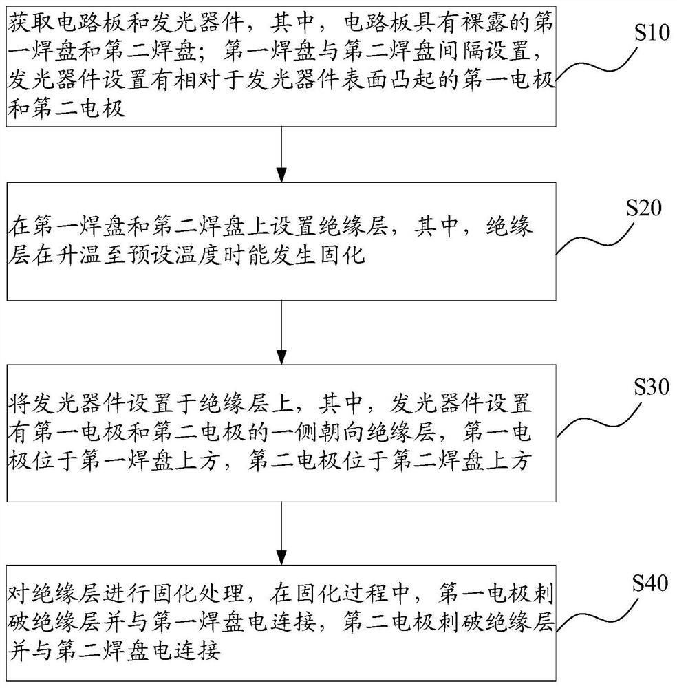
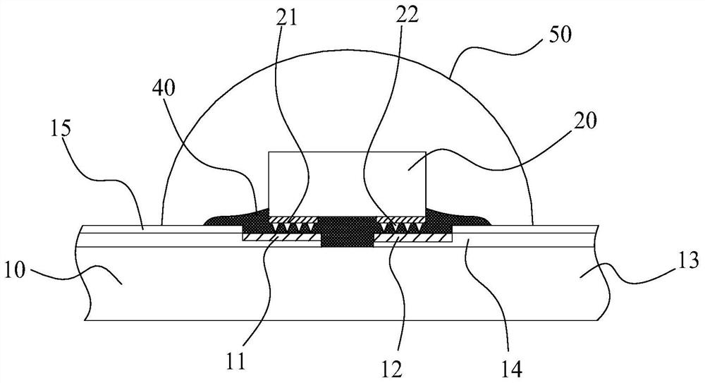
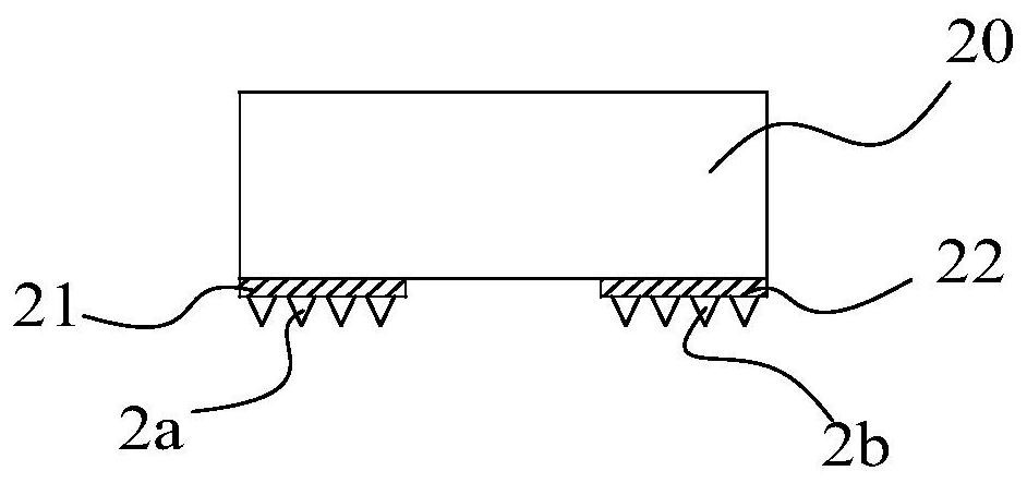
[0037] The technical solutions in the embodiments of the present application will be clearly and completely described below in conjunction with the drawings in the embodiments of the present application. Apparently, the described embodiments are only some of the embodiments of this application, not all of them. The following description of at least one exemplary embodiment is merely illustrative in nature and in no way serves as any limitation of the application, its application or uses. Based on the embodiments in this application, all other embodiments obtained by those skilled in the art without making creative efforts belong to the protection scope of this application.

[0038] Reference herein to "an embodiment" or "implementation" means that a particular feature, component or characteristic described in connection with the embodiment or implementation may be included in at least one embodiment of the present application. The occurrences of this phrase in various places ...


PUM

PropertyMeasurementUnit
thicknessaaaaaaaaaa
transmittivityaaaaaaaaaa
refractive indexaaaaaaaaaa

Abstract

The invention provides a preparation method of a backlight source. The preparation method comprises the following steps that: a circuit board and a light emitting device are obtained, wherein the circuit board has a first bonding pad and a second bonding pad which are exposed; the first bonding pad and the second bonding pad are arranged at an interval, and the light emitting device is provided with a first electrode and a second electrode which protrude relative to the surface of the light emitting device; an insulating layer is arranged on the first bonding pad and the second bonding pad, and the insulating layer can be solidified when the temperature rises to a preset temperature; the light emitting device is arranged on the insulating layer, the side, provided with the first electrode and the second electrode, of the light emitting device faces the insulating layer, the first electrode is located above the first bonding pad, and the second electrode is located above the second bonding pad; and the insulating layer is cured, in the curing process, the first electrode punctures the insulating layer and is electrically connected with the first bonding pad, and the second electrode punctures the insulating layer and is electrically connected with the second bonding pad. With the preparation method of the backlight source adopted, the problems that an LED chip is low in die bonding yieldand high in repair rate when an existing backlight source is manufactured can be solved.

Description

technical field [0001] The present application relates to the field of display technology, in particular to a method for preparing a backlight source. Background technique [0002] Mini LED (Mini Light-Emitting Diode, Mini-LED) backlight is a kind of LCD display backlight emerging in recent years. Mini LED backlight is to arrange a plurality of Mini LED chip arrays on the printed circuit board, and the LED light-emitting surface is far away from the printed circuit board. The Mini LED backlight can realize the switching of LED chips in different regions, that is, Local Dimming (regional dimming), which can greatly improve the contrast of the LCD display and enhance the image quality of the LCD display. [0003] Among them, the chip usually used in the Mini LED backlight is an LED chip with a flip-chip structure. The LED chip is provided with a pad. The die-bonding method is usually to print solder paste on the pad of the printed circuit board, and then use a die-bonding mac...

Claims


Application Information

Patent Timeline
Patent Type & Authority Applications(China)
IPC IPC(8): H05K3/34G02F1/1333G02F1/13357
CPCH05K3/3421H05K3/3457G02F1/1333G02F1/133605G02F1/133607G02F1/133612
Inventor 桑永昌李健林
Owner HUIZHOU VISION NEW TECH CO LTD
Why Eureka
Try Eureka