Array substrate, manufacturing method thereof and display panel

Active Publication Date: 2022-03-01
WUHAN CHINA STAR OPTOELECTRONICS SEMICON DISPLAY TECH CO LTD
View PDF5 Cites 0 Cited by
  • Summary
  • Abstract
  • Description
  • Claims
  • Application Information

AI Technical Summary

Problems solved by technology

However, limited by the process line width and wiring of thin film transistors, the development of high-resolution display devices is limited

Method used


Image

  • Array substrate, manufacturing method thereof and display panel
  • Array substrate, manufacturing method thereof and display panel
  • Array substrate, manufacturing method thereof and display panel

Examples


Embodiment Construction

[0032] The technical solutions in the embodiments of the present application will be clearly and completely described below in conjunction with the drawings in the embodiments of the present application. Apparently, the described embodiments are only some of the embodiments of this application, not all of them. Based on the embodiments in this application, all other embodiments obtained by those skilled in the art without making creative efforts belong to the scope of protection of this application.

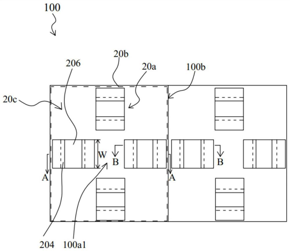
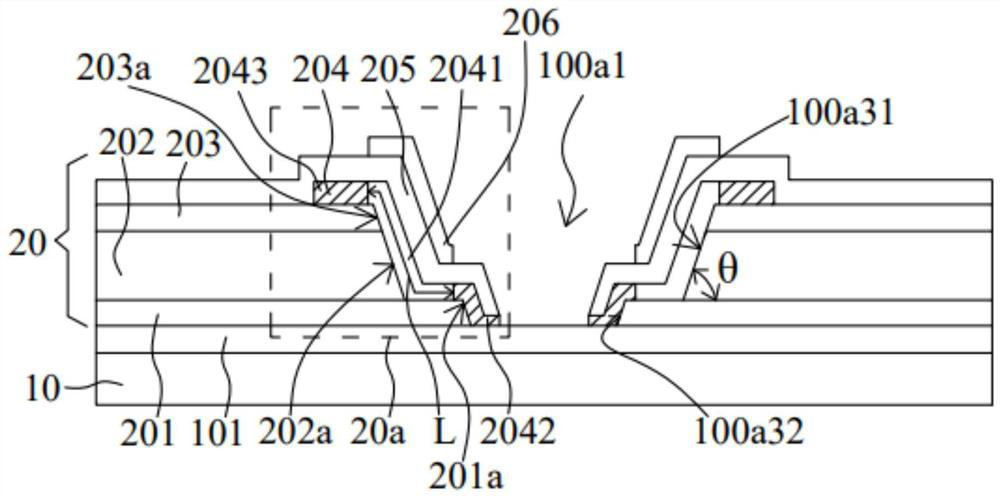
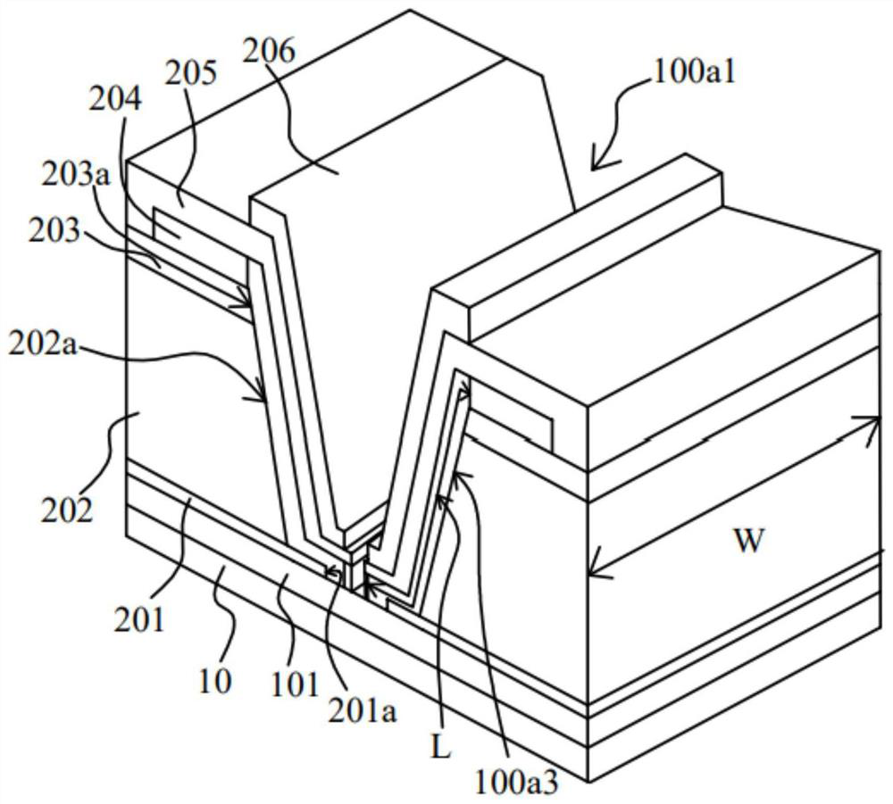
[0033] At present, since the active layer of the vertical thin film transistor extends along the thickness direction of the array substrate, the vertical thin film transistor occupies a small space in the horizontal direction. By utilizing the feature that the vertical thin film transistor occupies a small horizontal space, it can The number of thin film transistors per unit area in the horizontal direction is increased. However, there is no corresponding design in the prior art...


PUM

PropertyMeasurementUnit
thicknessaaaaaaaaaa
thicknessaaaaaaaaaa
thicknessaaaaaaaaaa

Abstract

The invention discloses an array substrate, a manufacturing method of the array substrate and a display panel. The first thin film transistor layer is arranged on the substrate, the first thin film transistor layer comprises a plurality of spaced first thin film transistors, and each first thin film transistor comprises a first electrode with a first side wall; a second electrode having a second sidewall; a first active pattern extending in a thickness direction of the array substrate; the first grid electrode extends in the thickness direction of the array substrate and is located on the side, away from the first electrode and the second electrode, of the first active pattern in the direction perpendicular to the thickness direction of the array substrate. The at least one first opening penetrates through the first thin film transistor layer; the first electrodes and the second electrodes of the at least two first thin film transistors are arranged around a first opening, and the first opening comprises the first side walls of the first electrodes of the at least two first thin film transistors and the second side walls of the second electrodes of the at least two first thin film transistors.

Description

technical field [0001] The present application relates to the field of display technology, in particular to an array substrate, a manufacturing method thereof, and a display panel. Background technique [0002] In recent years, high-resolution display devices are the development trend in the display field. The resolution (Pixel per inch, PPI) of the display panel is related to the pixel aperture ratio of the array substrate, and the pixel aperture ratio of the array substrate is related to the size and unit area of ​​the thin film transistor. The number of thin film transistors is related. The larger the area occupied by the thin film transistors, the lower the pixel aperture ratio and the lower the resolution of the display panel. However, the development of high-resolution display devices is limited by the limitation of the process line width and wiring of thin film transistors. [0003] Therefore, it is necessary to propose a technical solution to improve the resolution ...

Claims


Application Information

Patent Timeline
Patent Type & Authority Applications(China)
IPC IPC(8): H01L27/12H01L21/77
CPCH01L27/124H01L27/1248H01L27/1222H01L27/1259H01L27/127
Inventor 沈海燕郑辉黄灿鲜于文旭张春鹏
Owner WUHAN CHINA STAR OPTOELECTRONICS SEMICON DISPLAY TECH CO LTD
Why Eureka
Try Eureka