Unlock instant, AI-driven research and patent intelligence for your innovation.

NAND flash memory structure and manufacturing method thereof

A manufacturing method and technology of flash memory, applied in the direction of electrical components, electrical solid devices, circuits, etc., can solve problems affecting the area of ​​the device area, and achieve the effect of saving area

Pending Publication Date: 2022-04-12
SHANGHAI HUALI MICROELECTRONICS CORP
View PDF0 Cites 0 Cited by
  • Summary
  • Abstract
  • Description
  • Claims
  • Application Information

AI Technical Summary

Problems solved by technology

[0003] The object of the present invention is to provide a kind of NAND flash memory structure and its manufacturing method, to solve the problem that the source selection gate, the drain selection gate and the word line have different critical dimensions and affect the area of ​​the device region

Method used


Image

  • NAND flash memory structure and manufacturing method thereof
  • NAND flash memory structure and manufacturing method thereof
  • NAND flash memory structure and manufacturing method thereof

Examples


Embodiment Construction

[0026] A NAND flash memory structure and its manufacturing method proposed by the present invention will be further described in detail below in conjunction with the accompanying drawings and specific embodiments. Advantages and features of the present invention will be apparent from the following description and claims. It should be noted that all the drawings are in a very simplified form and use imprecise scales, and are only used to facilitate and clearly assist the purpose of illustrating the embodiments of the present invention.

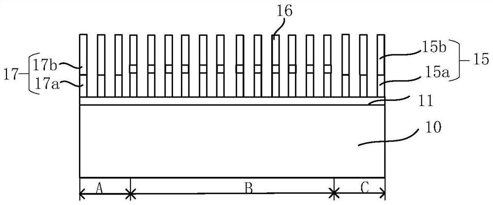
[0027] Specifically, please refer to figure 1 , which is a schematic structural diagram of a NAND flash memory according to an embodiment of the present invention. Such as figure 1 As shown, the present invention provides a NAND flash memory structure, including: a substrate 10, on which a plurality of word lines 16, a plurality of source selection gates 17 and a plurality of drain selection gates 15 are formed, A plurality of word lines 16 ...


PUM


Abstract

The invention provides an NAND flash memory structure, which comprises a substrate, a plurality of word lines, a plurality of source selection grids and a plurality of drain selection grids are formed on the substrate, the plurality of word lines are positioned between the plurality of source selection grids and the plurality of drain selection grids, and the widths of each word line, each source selection grid and each drain selection grid are the same. By forming the source selection gate, the drain selection gate and the word line with the same width, the width of the word line is the same as the width of the source selection gate and the width of the drain selection gate, so that a load effect is not generated, and the word line close to the source selection gate and the drain selection gate does not need to be set as a redundant word line; therefore, the area of the device region is saved.

Description

technical field [0001] The invention relates to the technical field of semiconductors, in particular to a NAND flash memory structure and a manufacturing method thereof. Background technique [0002] In the existing NAND FLASH structure, many word lines (word lines, WL) are connected in series between a drain selective gate (DSG) and a source selective gate (SSG). Because the source selection gate, drain selection gate and word line have different critical dimensions (Critical Dimension, CD), there will be a loading effect (loading effect), close to the source selection gate or drain selection gate Word lines have different sizes and shapes, and cannot be used as word lines, but can only be used as dummy WLs, which affects the area of ​​the device (cell) region. Contents of the invention [0003] The purpose of the present invention is to provide a NAND flash memory structure and its manufacturing method, so as to solve the problem that the different critical dimensions o...

Claims


Application Information

Patent Timeline
Patent Type & Authority Applications(China)
IPC IPC(8): H01L27/11524H10B41/35
Inventor 刘涛巨晓华王奇伟
Owner SHANGHAI HUALI MICROELECTRONICS CORP