Power semiconductor device

A semiconductor and power technology, applied in the direction of semiconductor devices, circuits, electrical components, etc., can solve the problems of depletion layer elongation obstruction, withstand voltage drop, variation, etc., to achieve the effect of suppressing the drop of withstand voltage

Pending Publication Date: 2022-04-22
MITSUBISHI ELECTRIC CORP
View PDF1 Cites 0 Cited by
  • Summary
  • Abstract
  • Description
  • Claims
  • Application Information

AI Technical Summary

Problems solved by technology

[0004] However, there is a problem that since the semi-insulating film has fixed charges, the carrier concentration in the termination region fluctuates, thereby hindering the elongation of the depletion layer when a reverse bias is applied, resulting in a decrease in withstand voltage.

Method used


Image

  • Power semiconductor device
  • Power semiconductor device
  • Power semiconductor device

Examples


Embodiment approach 1

[0024]

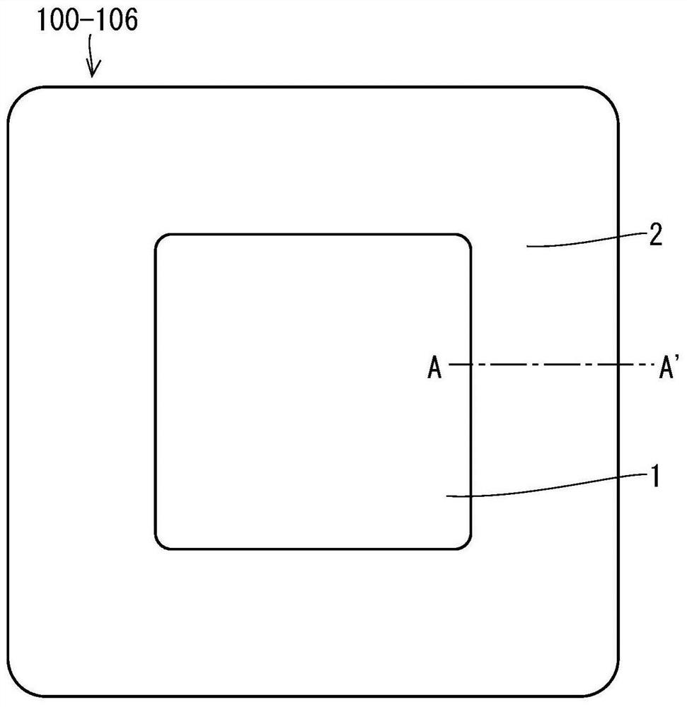
[0025] figure 1 It is a plan view of the power semiconductor device 101 according to the first embodiment. also, figure 1 The illustrated plan views are also used as plan views of the power semiconductor devices of the embodiments and the power semiconductor devices of the comparative examples described later. Such as figure 1 As shown, the power semiconductor device 101 is configured to have a cell region 1 and a termination region 2 surrounding the cell region 1 .

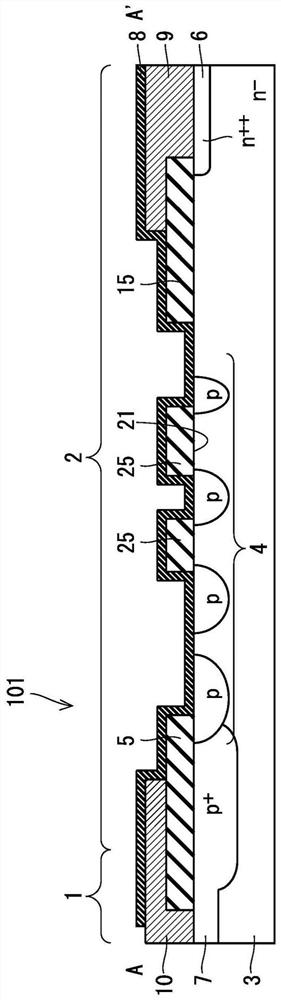
[0026] figure 2 is along figure 1 A cross-sectional view of the power semiconductor device 101 taken along the line A-A'. Such as figure 2 As shown, the power semiconductor device 101 is divided into a cell region 1 and a terminal region 2 when viewed from above, and the power semiconductor device 101 has an n-type semiconductor substrate 3, insulating films 5, 15, n++ type diffusion layers 6, p+ type diffusion layer 7, semi-insulating film 8, electrodes 9, 10 and at least one p-type diffusion...

Embodiment approach 2

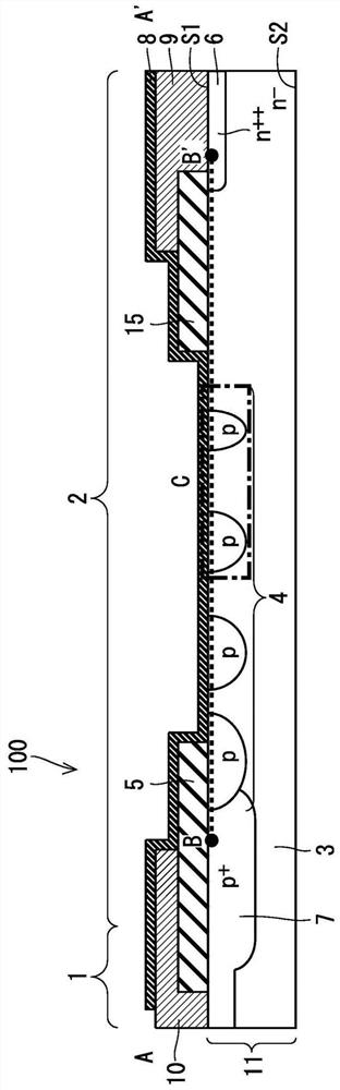
[0052] Figure 8 It is the edge of the power semiconductor device 102 of Embodiment 2. figure 1 A cross-sectional view of line A-A'. The power semiconductor device 102 differs from the power semiconductor device 101 only in the arrangement of the insulating film 25 and the contact form between the semi-insulating film 8 and the semiconductor base 11 accompanying the arrangement. Hereinafter, only the parts different from those of the power semiconductor device 101 in the structure of the power semiconductor device 102 will be described.

[0053] In the power semiconductor device 102 , the insulating film 25 is formed on a region of the substrate exposed region 21 excluding both ends in contact with the p-type diffusion layer 4 . Therefore, semi-insulating film 8 is in contact with p-type diffusion layer 4 and the end of substrate exposed region 21 in contact with p-type diffusion layer 4 .

[0054] That is, in the power semiconductor device 102 according to Embodiment 2, th...

Embodiment approach 3

[0056] Figure 9 It is the edge of the power semiconductor device 103 according to the third embodiment. figure 1 A cross-sectional view of line A-A'. The power semiconductor device 103 differs from the power semiconductor device 101 only in the arrangement of the insulating film 25 and the contact form between the semi-insulating film 8 and the semiconductor base 11 accompanying the arrangement. Hereinafter, only the parts different from those of the power semiconductor device 101 in the structure of the power semiconductor device 103 will be described.

[0057] In the power semiconductor device 103 , the insulating film 25 is formed across the entire exposed substrate region 21 and end regions of the p-type diffusion layer 4 adjacent to both sides of the exposed substrate region 21 . Therefore, the semi-insulating film 8 is in contact only with the p-type diffusion layer 4 on the first main surface S1 of the semiconductor base 11 , and is not in contact with the semiconduc...


PUM


Abstract

The purpose of the present invention is to suppress a drop in withstand voltage of a power semiconductor device. A semiconductor base (11) has: an n-type semiconductor substrate (3); and at least one p-type diffusion layer (4) which is formed so as to be separated from each other on a surface layer on the first main surface (S1) side of the semiconductor substrate (3) in the termination region (2). The power semiconductor device (101) has at least one insulating film (25) formed on the first main surface (S1) of the semiconductor base body (11) between the insulating films (5, 15). The semi-insulating film (8) is in contact with the insulating film (25) on the insulating film (25), and is in contact with the first main surface (S1) in at least two or more regions between the insulating films (5, 15) in which the insulating film (25) is not formed.

Description

technical field [0001] The present invention relates to a semiconductor device for electric power. Background technique [0002] Generally, a power semiconductor device has a cell region and a terminal region surrounding the cell region. In some cases, a power semiconductor device has a semi-insulating film that connects electrodes formed in the cell region and electrodes formed on the outer peripheral side of the terminal region. This semi-insulating film is in direct contact with the surface of the Si semiconductor substrate in the termination region, and has the function of allowing carriers generated in the termination region to flow to the electrodes when a reverse bias is applied. This suppresses the carriers from being captured by the insulating film, suppresses the carrier concentration from fluctuating on the surface of the semiconductor substrate in the termination region, and prevents the elongation of the depletion layer when a reverse bias is applied. As a res...

Claims


Application Information

Patent Timeline
Patent Type & Authority Applications(China)
IPC IPC(8): H01L29/06
CPCH01L29/0611H01L29/0615H01L29/0619H01L29/0623H01L29/8611H01L29/405H01L29/0638
Inventor 原口友树增冈史仁陈则
Owner MITSUBISHI ELECTRIC CORP
Why Eureka
Try Eureka