Superjunction semiconductor device and method of manufacturing superjunction semiconductor device

A technology of superjunction semiconductor and manufacturing method, applied in semiconductor/solid-state device manufacturing, semiconductor devices, electrical components, etc., can solve the problems of reduced withstand voltage, increased n-type drift layer, shortened depletion layer expansion distance, etc.

Pending Publication Date: 2020-10-23
FUJI ELECTRIC CO LTD
View PDF3 Cites 0 Cited by
  • Summary
  • Abstract
  • Description
  • Claims
  • Application Information

AI Technical Summary

Problems solved by technology

Therefore, in the case of thinning the n-type drift layer in order to reduce the on-state resistance, the extension distance of the depletion layer in the off state will be shortened, so it is easy to reach the breakdown electric field strength at a low applied voltage, making the withstand voltage reduce
On the other hand, in order to improve the withstand voltage of the vertical MOSFET, it is necessary to increase the thickness of the n-type drift layer to increase the on-state resistance
Such a relationship between on-state resistance and withstand voltage is called a trade-off relationship, and it is generally difficult to improve both of them in the trade-off relationship.

Method used


Image

  • Superjunction semiconductor device and method of manufacturing superjunction semiconductor device
  • Superjunction semiconductor device and method of manufacturing superjunction semiconductor device
  • Superjunction semiconductor device and method of manufacturing superjunction semiconductor device

Examples


Embodiment approach 1

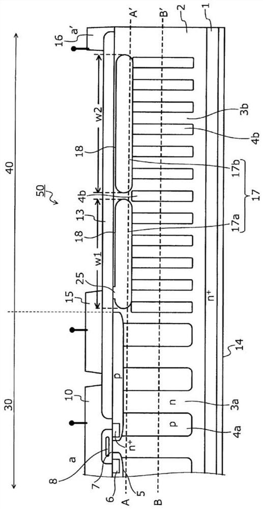
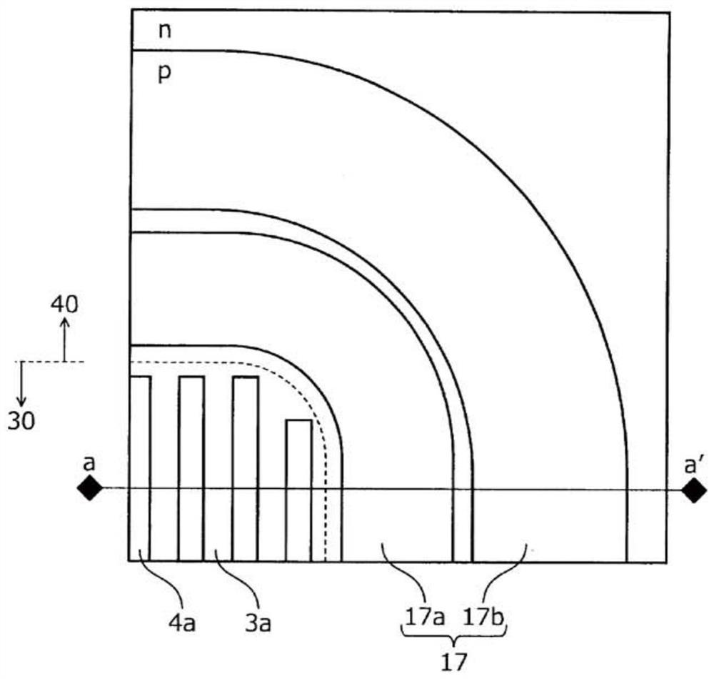
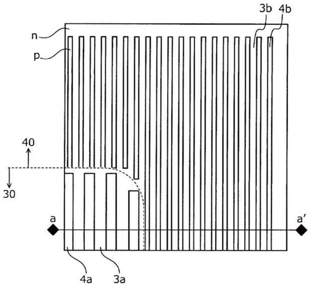
[0111] The super junction semiconductor device of the present invention will be described by taking the SJ-MOSFET as an example. figure 1 It is a cross-sectional view showing the structure of the SJ-MOSFET of the first embodiment. figure 2 shows the structure of the SJ-MOSFET of Embodiment 1 figure 1 A top view of part A-A' of . in addition, image 3 shows the structure of the SJ-MOSFET of Embodiment 1 figure 1 Top view of part B-B' of . in addition, Figure 4 shows the structure of the SJ-MOSFET of Embodiment 1 figure 1 Another top view of part B-B' of . figure 1 Yes Figure 2 ~ Figure 4 A cross-sectional view of part a-a' of .

[0112] figure 1 The shown SJ-MOSFET 50 is equipped with a MOS (Metal Oxide Semiconductor: Metal Oxide Semiconductor) on the front side (the surface on the side of the p-type base region 5 described later) of a semiconductor substrate (silicon substrate: semiconductor chip) including silicon (Si). ) gate of the SJ-MOSFET50. This SJ-M...

Embodiment approach 2

[0127] Figure 5 is a cross-sectional view showing the structure of the SJ-MOSFET of the second embodiment. Figure 5 The A-A' part is the same as that showing the structure of the SJ-MOSFET of the first embodiment figure 2 The same part of the top view. In addition, the structure of the SJ-MOSFET of Embodiment 2 is shown Figure 5 The B-B' part is the same as that showing the structure of the SJ-MOSFET of the first embodiment image 3 The same part of the top view. In addition, the structure of the SJ-MOSFET of Embodiment 2 is shown Figure 5 Other top view of the B-B' section with Figure 4 same top view.

[0128] Embodiment 2 is different in that no p-type P-type device not connected to the first Resurf region 17a and the second Resurf region 17b is arranged between the first Resurf region 17a and the second Resurf region 17b. Column area 4b.

[0129] Embodiment 2 Even if the p-type column region 4b not connected to the first resurf region 17a and the second resurf...

Embodiment approach 3

[0161] Figure 14 It is a cross-sectional view showing the structure of the SJ-MOSFET of the third embodiment. Embodiment 3 differs from Embodiments 1 and 2 in that the RESURF region 17 is divided into a first RESURF region 17a, a second RESURF region 17b, a third RESURF region 17c, and a second RESURF region 17a. The four RESURF regions 17d are the four.

[0162] In Embodiment Mode 3, the width w1 of the first resurf region 17a, the width w2 of the second resurf region 17b, the width w3 of the third resurf region 17c, and the width w4 of the fourth resurf region 17d are preferably There is a relationship of w1≤w2≤w3≤w4. exist Figure 14 Among them, the end 25 of the first resurf region 17a is a part of the p-type base region 5 , and the first resurf region 17a can be connected to the field plate electrode 15a through the p-type base region 5 . Similarly, the second RESURF region 17b, the third RESURF region 17c, and the fourth RESURF region 17d can also be connected to th...


PUM


Abstract

The invention provides a superjunction semiconductor device and a method of manufacturing the superjunction semiconductor device, which can restrain voltage resistance reduction caused by manufacturing deviation. The semiconductor device has an active region (30) through which current flows and a termination structure region (40). On a front surface of a semiconductor substrate (1) of a first conductivity type, a first semiconductor layer (2) of the first conductivity type is provided. On a surface of the first semiconductor layer (2) in the active region (30), a first parallel pn structure isprovided including first columns (3a) of the first conductivity type and second columns (4a) of a second conductivity type disposed repeatedly alternating one another in a plane parallel to the frontsurface. In the termination structure region (40), a second parallel pn structure is provided including third columns (3b) of the first conductivity type and fourth columns (4b) of the second conductivity type disposed repeatedly alternating one another. On a surface of the second parallel pn structure, a first semiconductor region (17) of the second conductivity type is provided including pluralregions apart from one another.

Description

technical field [0001] The present invention relates to a super junction semiconductor device and a method for manufacturing the super junction semiconductor device. Background technique [0002] In a normal n-channel vertical MOSFET (Metal Oxide Semiconductor Field Effect Transistor: Insulated Gate Field Effect Transistor), among the multiple semiconductor layers formed in the semiconductor substrate, the n-type conduction layer (drift layer) has the highest resistance semiconductor layer. The resistance of the n-type drift layer greatly affects the on-state resistance of the entire vertical MOSFET. The on-resistance of the entire vertical MOSFET can be reduced by reducing the thickness of the n-type drift layer and shortening the current path. [0003] However, the vertical MOSFET also has a function of maintaining a breakdown voltage by extending the depletion layer to the high-resistance n-type drift layer in the off state. Therefore, in the case of thinning the n-typ...

Claims


Application Information

Patent Timeline
IPC IPC(8): H01L29/06H01L29/78H01L21/336
CPCH01L29/0634H01L29/0684H01L29/7828H01L29/66666
Inventor 坂田敏明
Owner FUJI ELECTRIC CO LTD
Why Eureka
Try Eureka