Power semiconductor device

Pending Publication Date: 2022-04-28
MITSUBISHI ELECTRIC CORP
View PDF1 Cites 0 Cited by
  • Summary
  • Abstract
  • Description
  • Claims
  • Application Information

AI Technical Summary

Benefits of technology

The patent text aims to address a problem in power semiconductor devices where the fixed charge in the semi-insulating film can affect the carrier concentration and prevent the depletion layer from extending when a reverse bias is applied, which in turn reduces the withstand voltage. The technical effect of this patent is to suppress the reduction of withstand voltage in power semiconductor devices.

Problems solved by technology

However, the semi-insulating film has a fixed charge, thus there is a problem that the fixed charge varies the carrier concentration in the terminal region, thereby inhibiting the extension of the depletion layer at the time of applying the reverse bias and reducing the withstand voltage.

Method used


Image

  • Power semiconductor device
  • Power semiconductor device
  • Power semiconductor device

Examples


embodiment 1

A. EMBODIMENT 1

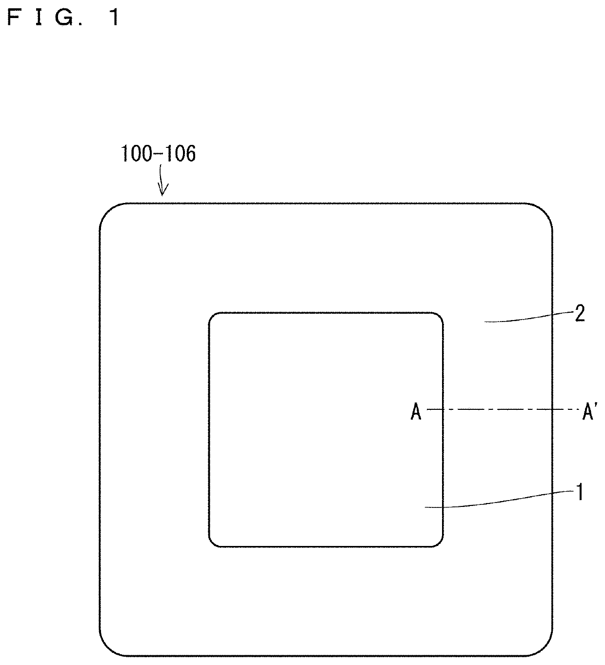
[0022]FIG. 1 is a plan view of a power semiconductor device 101 according to an embodiment 1. The plan view illustrated in FIG. 1 is also used as a plan view of a power semiconductor device according to each embodiment described hereinafter and a power semiconductor device of a comparison example. As illustrated in FIG. 1, the power semiconductor device 101 includes a cell region 1 and a terminal region 2 surrounding the cell region 1.

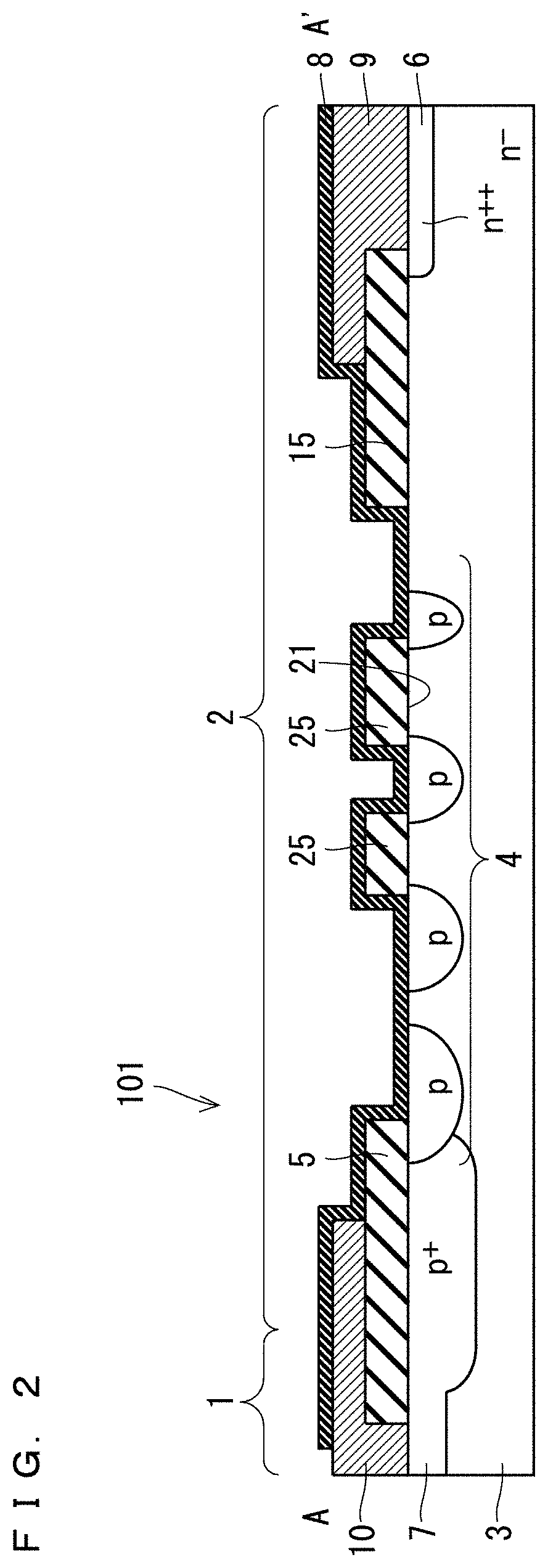
[0023]FIG. 2 is a cross-sectional view of the power semiconductor device 101 along an A-A′ line in FIG. 1. As illustrated in FIG. 2, the power semiconductor device 101 is divided into the cell region 1 and the terminal region 2 in a plan view, and includes a n− type semiconductor substrate 3, at least one p type diffusion layer 4, insulating films 5 and 15, an n++ type diffusion layer 6, a p+ type diffusion layer 7, a semi-insulating film 8, and electrodes 9 and 10.

[0024]The n− type semiconductor substrate 3, at least one p type diffusio...

embodiment 2

B. EMBODIMENT 2

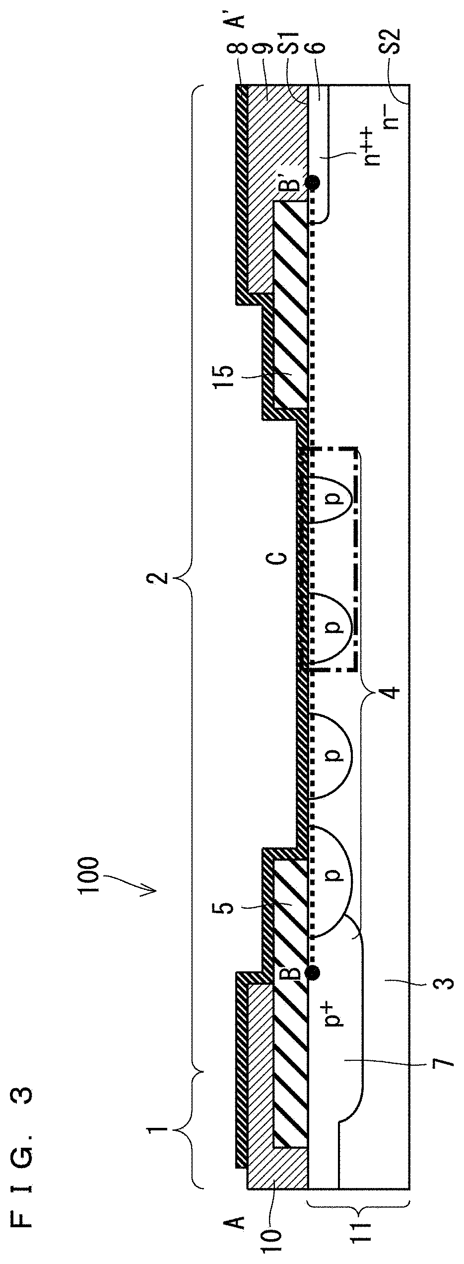
[0047]FIG. 8 is a cross-sectional view of a power semiconductor device 102 of an embodiment 2 along the A-A′ line in FIG. 1. Only an arrangement of the insulating film 25 and a contact form of the semi-insulating film 8 with the semiconductor base 11 in accordance with the arrangement thereof are different between the power semiconductor device 102 and the power semiconductor device 101. Only a part of a configuration of the power semiconductor device 102 different from that of the power semiconductor device 101 is described hereinafter.

[0048]In the power semiconductor device 102, the insulating film 25 is formed on a region in the substrate exposed region 21 except for both end portions thereof having contact with the p type diffusion layer 4. Accordingly, the semi-insulating film 8 has contact with the p type diffusion layer 4 and an end portion of the substrate exposed region 21 having contact with the p type diffusion layer 4.

[0049]That is to say, in the power sem...

embodiment 3

C. EMBODIMENT 3

[0050]FIG. 9 is a cross-sectional view of a power semiconductor device 103 of an embodiment 3 along the A-A′ line in FIG. 1. Only an arrangement of the insulating film 25 and a contact form of the semi-insulating film 8 with the semiconductor base 11 in accordance with the arrangement thereof are different between the power semiconductor device 103 and the power semiconductor device 101. Only a part of a configuration of the power semiconductor device 103 different from that of the power semiconductor device 101 is described hereinafter.

[0051]In the power semiconductor device 103, the insulating film 25 is formed to extend across all the substrate exposed regions 21 and the end portion region of the p type diffusion layers 4 adjacent to the both sides of the substrate exposed region 21. Accordingly, the semi-insulating film 8 has contact with only the p type diffusion layer 4 in the first main surface S1 of the semiconductor base 11, and does not have contact with the...


PUM


Abstract

An object of a technique of the present disclosure is to suppress reduction in withstand voltage in a power semiconductor device. A semiconductor base includes an n− type semiconductor substrate and at least one p type diffusion layer formed separately from each other on a surface layer on a side of a first main surface of the semiconductor substrate in a terminal region. A power semiconductor device includes at least one insulating film formed on a first main surface of the semiconductor base between an insulating film and the insulating film. A semi-insulating film has contact with the insulating film on the insulating film, and has contact with the first main surface in at least two regions where the insulating film is not formed between the insulating films and.

Description

BACKGROUND OF THE INVENTIONField of the Invention[0001]The present disclosure relates to a power semiconductor device.Description of the Background Art[0002]A power semiconductor device generally includes a cell region and a terminal region surrounding the cell region. A power semiconductor device includes a semi-insulating film connecting an electrode formed in a cell region and an electrode formed on an outer peripheral side of a terminal region in some cases. The semi-insulating film has a role of directly having contact with a surface of an Si semiconductor substrate in the terminal region to flow a carrier generated in the terminal region at a time of applying a reverse bias to the electrode. Accordingly, the carrier is prevented from being trapped by the insulating film, and also suppressed are a variation of a carrier concentration in a surface of a semiconductor substrate of a terminal region and inhibition of an extension of a depletion layer at the time of applying the rev...

Claims


Application Information

Patent Timeline
IPC IPC(8): H01L29/06
CPCH01L29/0623H01L29/0611H01L29/0615H01L29/0619H01L29/8611H01L29/405H01L29/0638
Inventor HARAGUCHI, YUKIMASUOKA, FUMIHITOCHEN, ZE
Owner MITSUBISHI ELECTRIC CORP
Why Eureka
Try Eureka