Semiconductor device having a gate oxide film with some NTFTS with LDD regions and no PTFTS with LDD regions

a technology of metal insulator and gate oxide film, which is applied in the direction of semiconductor devices, semiconductor/solid-state device details, electrical equipment, etc., can solve the problems of increasing leak current (off current), remarkably large electric field, and requiring crystallinity improvement (activation). improve the insulating quality, reduce the coupling capacity, and the effect of high withstanding voltag

Inactive Publication Date: 2006-02-07
SEMICON ENERGY LAB CO LTD
View PDF109 Cites 22 Cited by
  • Summary
  • Abstract
  • Description
  • Claims
  • Application Information

AI Technical Summary

Benefits of technology

[0019]Further, it goes without saying that, if necessary, the gate electrode can be anodized again in order to coat the surface thereof with an anodic oxide (a second anodic oxide) having a high insulating quality and an interlayer insulator or the like may be provided to lower a capacity coupling with an upper wire. It also goes without saying that although normally a wet method utilizing an electrolytic solution is used in the anodization, another known method of reduced pressure plasma (a dry method) may be used. Further, the anodic oxide obtained by the wet method may be a barrier type one which is minute and has a high withstanding voltage or a porous type one which is porous and has a low withstanding voltage. They may also be satisfactorily combined.

Problems solved by technology

However, the conventional process has a problem in that spatial changes of carrier density in the impurity region and in an active region (a channel forming region) which adjoins with the impurity region and is located under the gate electrode are too large, so that a remarkably large electric field is created and in particular, a leak current (OFF current) increases when an inverse bias voltage is applied to the gate electrode.
Further, because the crystallinity of a semiconductor substrate or semiconductor coating film is damaged in parts where ions have penetrated in methods such as the ion injecting method and plasma doping method, by which impurities are injected by radiating high speed ions onto the semiconductor substrate or semiconductor coating film, improvement (activation) of the crystallinity is required.
However, it was found that according to the method described above, the physical property at a boundary (indicated by X in FIG. 2C) between the impurity region and an active region (a semiconductor region sandwiched between the impurity regions directly under the gate electrode) is unstable and that problems could arise such as a leak current increasing over time and reliability decreasing.
It was then found that, although the impurity region is restored in the latter process of radiating laser beams, it is difficult to reproduce the same crystalline state as the original one and that the portion of the impurity region which contacts the active region in particular tends to be shaded during irradiation by laser beams and cannot be fully activated.
Then it is impossible to activate the region under the gate electrode section by laser beams or the like because it is shadowed by the gate electrode section.
However, the substrate material must transmit the light in this case and, as a matter of course, this method cannot be employed when a silicon wafer or the like is used.
Furthermore, because many glass substrates do not transmit ultraviolet light of less than 300 nm, a KrF excimer laser (wavelength: 248 nm), for example, which has excellent mass-producibility, cannot be utilized.

Method used


Image

  • Semiconductor device having a gate oxide film with some NTFTS with LDD regions and no PTFTS with LDD regions
  • Semiconductor device having a gate oxide film with some NTFTS with LDD regions and no PTFTS with LDD regions
  • Semiconductor device having a gate oxide film with some NTFTS with LDD regions and no PTFTS with LDD regions

Examples


first embodiment

[First Embodiment]

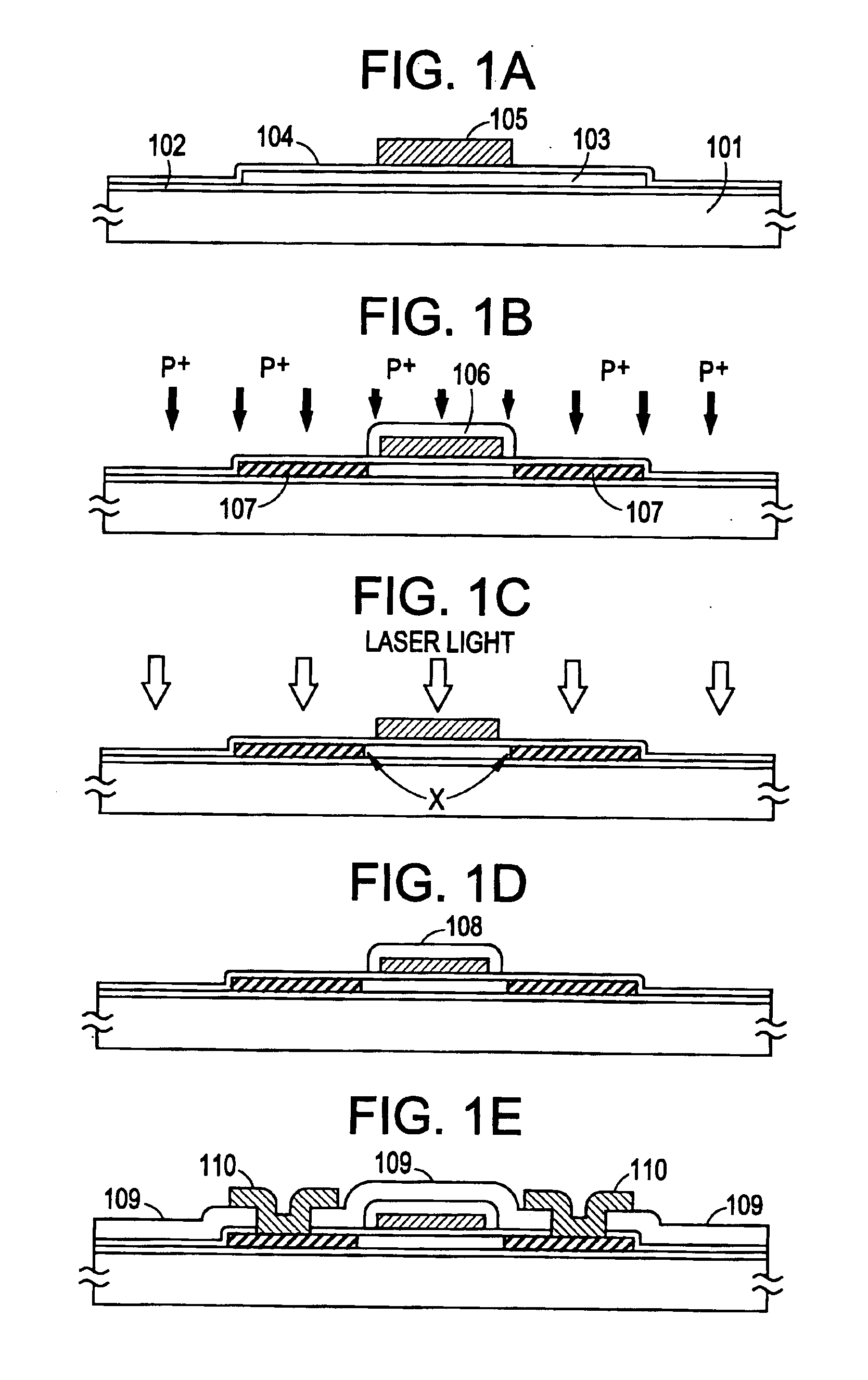
[0036]FIG. 1 shows a first preferred embodiment of the present invention. A thin film transistor is formed on an insulating substrate in this embodiment. The substrate 101 is a glass substrate, and a non-alkaline glass substrate such as Corning 7059 or a silica substrate, for example, may be used for the fabrication thereof. Taking costs into consideration, the Corning 7059 substrate was used here. A silicon oxide film 102 is deposited thereon as a ground oxide film. A sputtering method and a chemical vapor phase growing method (CVD method) may be used for depositing the silicon oxide film. The film was formed here by a plasma CVD method by using TEOS (tetraethoxisilane) and oxygen as material gases. The substrate temperature was 200 to 400° C. The thickness of the ground silicon oxide film was 500 to 2000 angstrom.

[0037]Next, an amorphous silicon film 103 was deposited and was patterned into a shape of island. A plasma CVD method and low pressure CVD method may be...

second embodiment

[Second Embodiment]

[0044]FIGS. 3 and 4 show a second embodiment. FIG. 3 is a section view taken along a dashed line in FIG. 4 (plan view). At first, a ground silicon oxide film was formed on a substrate (Corning 7059) 301 and an amorphous silicon film was formed to a thickness of 1000 to 1500 angstroms. Then the amorphous silicon film was crystallized by annealing at 600° C. for 24 to 48 hours in a nitrogen or argon atmosphere. A crystalline silicon island 302 was thus formed. Further, a silicon oxide film 303 which is 1000 angstroms thick and functions as a gate insulating film was deposited and tantalum wires (5000 angstroms thick) 304, 305 and 306 were formed (FIG. 3A).

[0045]Then a current was supplied to those wires 304 through 306 to form first anodic oxides 307, 308 and 309 having a thickness of 2000 to 2500 angstroms on the surface of those wires. Using those wires thus treated as a mask, impurities were injected into the silicon film 302 by means of a plasma doping method to...

third embodiment

[Third Embodiment]

[0050]FIG. 5 shows a third embodiment. A ground silicon oxide film was formed on a substrate (Corning 7059) 501 and an amorphous silicon film was formed to a thickness of 1000 to 1500 angstroms. Then the amorphous silicon film was crystallized by annealing it at 600° C. for 24 to 48 hours in a nitrogen or argon atmosphere. A crystalline silicon island 502 was thus formed. Further, a silicon oxide film 503 which is 1000 angstroms thick and functions as a gate insulating film was deposited and tantalum wires (5000 angstroms thick) 504, 505 and 506 were formed (FIG. 5A).

[0051]Then a current was circulated through those wires to form anodic oxide coating films 507, 508 and 509 having thicknesses of 500 to 1500 angstroms on the side and upper surfaces of those wires. Using those wires thus treated as a mask, impurities were injected into the silicon film 502 by means of a plasma doping method to form impurity regions 510 (FIG. 5B).

[0052]Then only the anodic oxides 507, ...


PUM


Abstract

A MIS type semiconductor device and a method for fabricating the same characterized in that impurity regions are selectively formed on a semiconductor substrate or semiconductor thin film and are activated by radiating laser beams or a strong light equivalent thereto from above so that the laser beams or the equivalent strong light are radiated onto the impurity regions and on an boundary between the impurity region and an active region adjoining the impurity region.

Description

[0001]This application is a Divisional of prior application Ser. No 08 / 855,143 filed May 13, 1997 now U.S. Pat. No. 6,489,632, which is a continuation of application Ser. No. 08 / 452,688 filed May 30, 1995, now abandoned, which is a divisional application of application Ser. No. 08 / 181,907 filed Jan. 18, 1994, now U.S. Pat. No. 5,627,084.BACKGROUND OF THE INVENTION[0002]1. Field of the Invention[0003]The present invention relates to a method for fabricating a metal insulator semiconductor type semiconductor device, i.e. a MIS type semiconductor device (also known as an insulated gate type semiconductor device). The MIS type semiconductor device includes, for example, a MOS transistor, thin film transistor and the like.[0004]2. Description of the Related Art[0005]Conventionally, a MIS type semiconductor device has been fabricated by using a self-aligning method. According to this method, a gate wiring (electrode) is formed on a semiconductor substrate or semiconductor coating film via...

Claims


Application Information

Patent Timeline
Patent Type & Authority Patents(United States)
IPC IPC(8): H01L23/62H01L29/04H01L31/036H01L21/20H01L21/00H01L21/336H01L21/77H01L21/84H01L29/08H01L29/78H01L29/786H01L31/00
CPCH01L29/66757H01L27/1285H01L27/124H01L29/78621H01L29/0847H01L29/7833H01L29/78681H01L29/78684
Inventor YAMAZAKI, SHUNPEITAKEMURA, YASUHIKO
Owner SEMICON ENERGY LAB CO LTD
Why Eureka
Try Eureka