SiC-MOSFET

a technology of mosfet and mosfet plate, which is applied in the direction of diodes, semiconductor devices, electrical apparatus, etc., can solve the problems of large number of stacking faults, significant deterioration of mosfet and so as to reduce the withstand voltage, and increase the current of the body diodes

Pending Publication Date: 2022-09-15
MITSUBISHI ELECTRIC CORP
View PDF0 Cites 0 Cited by
  • Summary
  • Abstract
  • Description
  • Claims
  • Application Information

AI Technical Summary

Benefits of technology

[0009]An object of a technique of the present disclosure is to suppress decrease i

Problems solved by technology

The stacking fault functions as a high resistance layer, thus when it extends, characteristics of the MOSFET and the body diode are deteriorated.
However, when the body diode current increases and the hole reaches the interface between the drift layer and the substrate, a large number of stacking faults extends from the fault in the substrate as a starting point.
The stacking fault functions as a high resistance layer, thus when it extends, characteristics of the MOSFET and the body diode are significantly deteriorated.
However, when the diode current increases to some degree, the body diode

Method used


Image

  • SiC-MOSFET
  • SiC-MOSFET
  • SiC-MOSFET

Examples


modification example

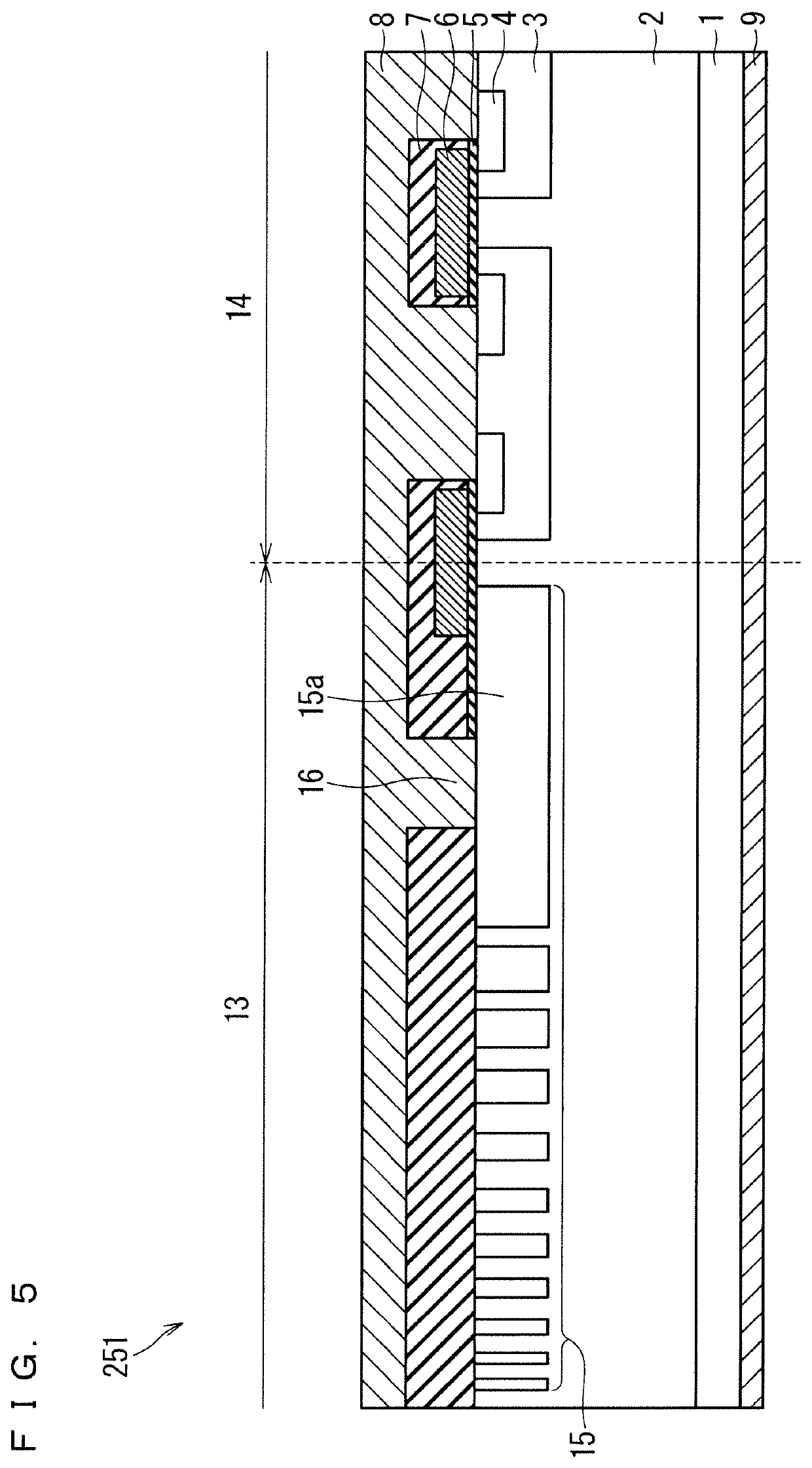
B-3. Modification Example

[0045]FIG. 7 is a cross-sectional view of an SiC-MOSFET 202 according to a first modification example of the embodiment 2. The SiC-MOSFET 202 is different from the SiC-MOSFET 201 according to the embodiment 2 in that the concave portion 12 is formed in the upper surface of the source region 4 in the active region 14 and the source contact portion of the base region 3 and the concave portion 22 is formed in the upper surface of the guard ring 15a on the innermost peripheral side in the outer peripheral region 13. The active region 14 of the SiC-MOSFET 202 has the same configuration as the SiC-MOSFET 102 according to the modification example of the embodiment 1. The gate insulating film 5, the interlayer insulating film 7, or the source electrode 8 is put into the concave portion 22.

[0046]FIG. 8 is a cross-sectional view of an SiC-MOSFET 203 according to a second modification example of the embodiment 2. In the SiC-MOSFET 203, the width of the concave portion ...


PUM


Abstract

An object of the present disclosure is to suppress decrease in withstand voltage and increase in ON voltage and to increase body diode current. An SiC-MOSFET includes: a source region formed on a surface layer of a base region; a gate electrode facing a channel region which is a region of the base region sandwiched between a drift layer and the source region via a gate insulating film; a source electrode having electrically contact with the source region; and a plurality of first embedded regions of a second conductivity type formed adjacent to a lower surface of the base region. The plurality of first embedded regions are formed immediately below at least both end portions of the base region, and three or more first embedded regions are formed to be separated from each other.

Description

BACKGROUND OF THE INVENTIONField of the Invention[0001]The present disclosure relates to an SiC-MOSFET.Description of the Background Art[0002]Widely used in a power electronic apparatus is an insulated gate type semiconductor device such as an insulated gate bipolar transistor (IGBT) or a metal oxide semiconductor field effect transistor (MOSFET) as a switching element controlling a power supply to a load such as a motor.[0003]There is a high degree of expectation in applying the MOSFET or the IGBT using a wide bandgap semiconductor such as silicon carbide (SiC) to a technical field dealing with high voltage of substantially 1 kV or more as a future switching element. Examples of the wide bandgap semiconductor include a gallium nitride series material and diamond in addition to silicon carbide.[0004]In a MOSFET having a vertical structure, a reverse pn diode referred to as a body diode is formed by a pn junction made up of an n-type drift layer and a p-type base region. The body dio...

Claims


Application Information

Patent Timeline
IPC IPC(8): H01L29/78H01L29/16H01L29/06H01L29/10
CPCH01L29/7805H01L29/1608H01L29/0623H01L29/0634H01L29/1095H01L29/7811H01L29/0692H01L29/7831H01L29/41766H01L29/0615H01L29/0619
Inventor SUGAWARA, KATSUTOSHIKAGAWA, YASUHIROFUKUI, YUTAKA
Owner MITSUBISHI ELECTRIC CORP
Why Eureka
Try Eureka