

Power semiconductor module
a technology of semiconductor modules and semiconductor elements, applied in semiconductor devices, semiconductor/solid-state device details, electrical apparatus, etc., can solve the problems the electric field cannot be relaxed enough, etc., to achieve the effect of reducing the ion concentration of silicone gel, reducing the risk of increasing the leakage current inside the semiconductor element, and maintaining the ability to relax the electric field for a long tim
- Summary
- Abstract
- Description
- Claims
- Application Information
AI Technical Summary
Benefits of technology
Problems solved by technology
Method used
Image

Examples
embodiment
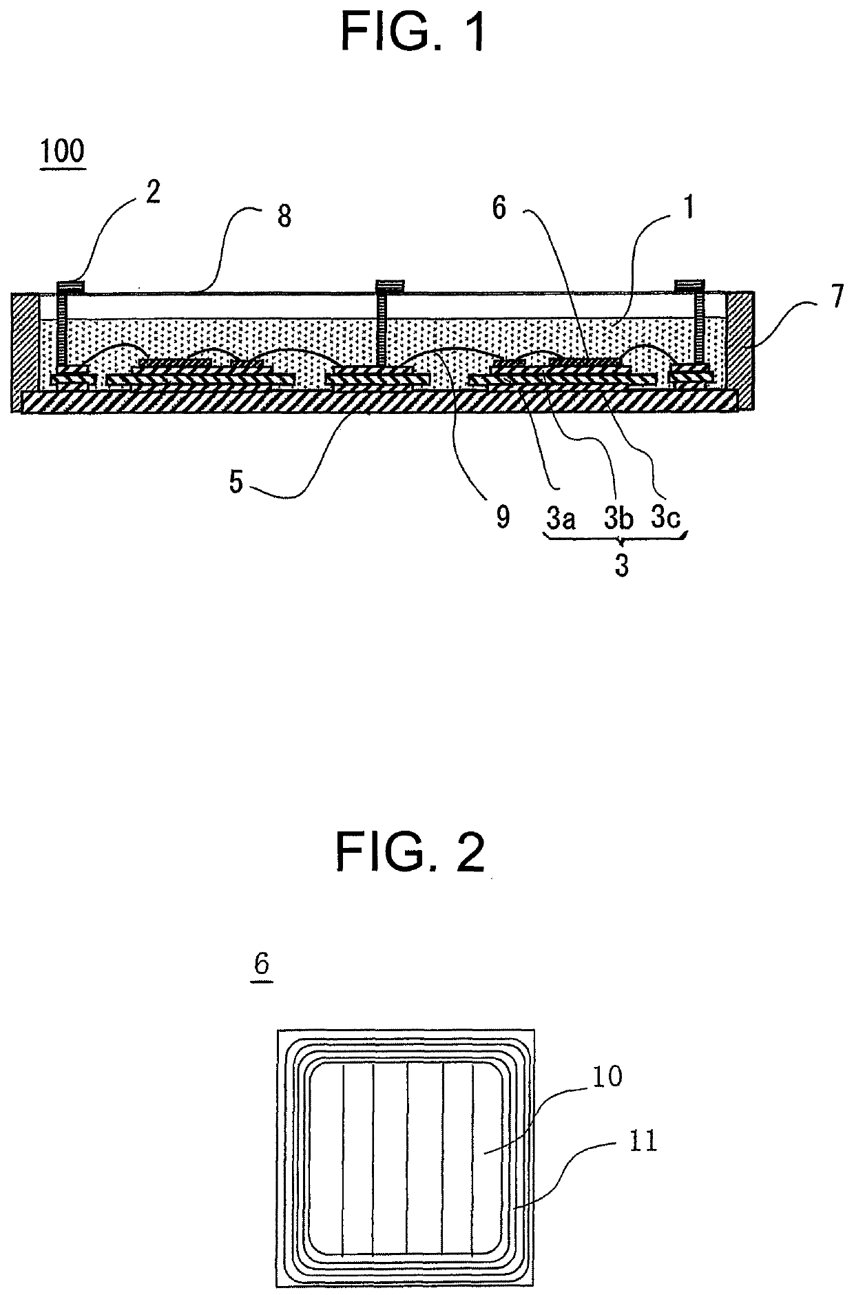
[0030]FIG. 1 is a cross-sectional view for illustrating a power semiconductor module according to one embodiment of the present invention. FIG. 2 is a top view for illustrating a semiconductor element in the power semiconductor module according to the one embodiment of the present invention.
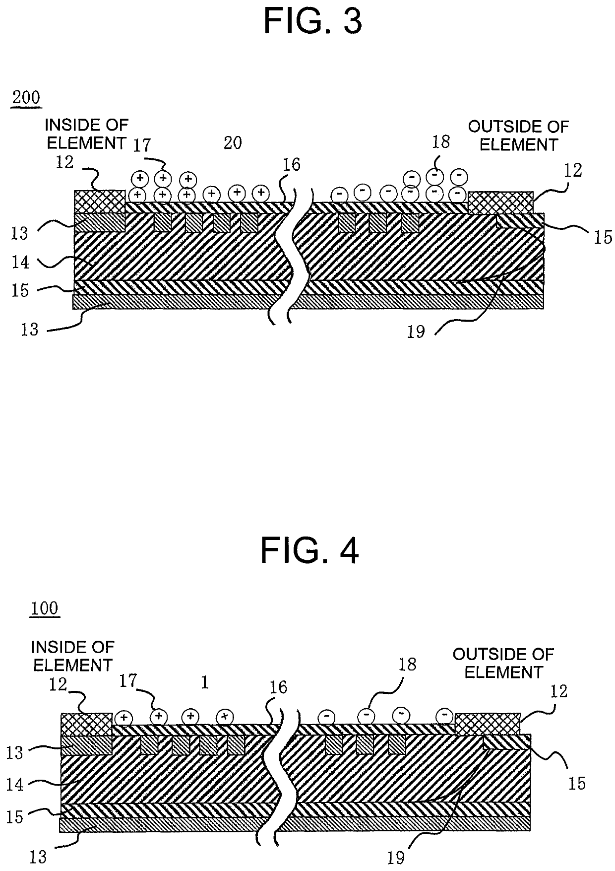
[0031]In FIG. 1, a power semiconductor module 100 includes: a metal base plate 5; a direct bond copper (DBC) substrate 3 arranged, by bonding, on the metal base plate 5; semiconductor elements 6 arranged, by bonding, on the DBC substrate 3; a plurality of external terminals 2 for electrical connection with any external part; a case 7 attached onto the metal base plate 5 so as to surround, for example, the external terminal 2, the DBC substrate 3, and the semiconductor elements 6; a potting material 1 filled into a space defined by the metal base plate 5 and the case 7 to seal the DBC substrate 3, the semiconductor elements 6, and other such components; and a cover 8 configured to cover an upper o...
PUM
| Property | Measurement | Unit |
|---|---|---|
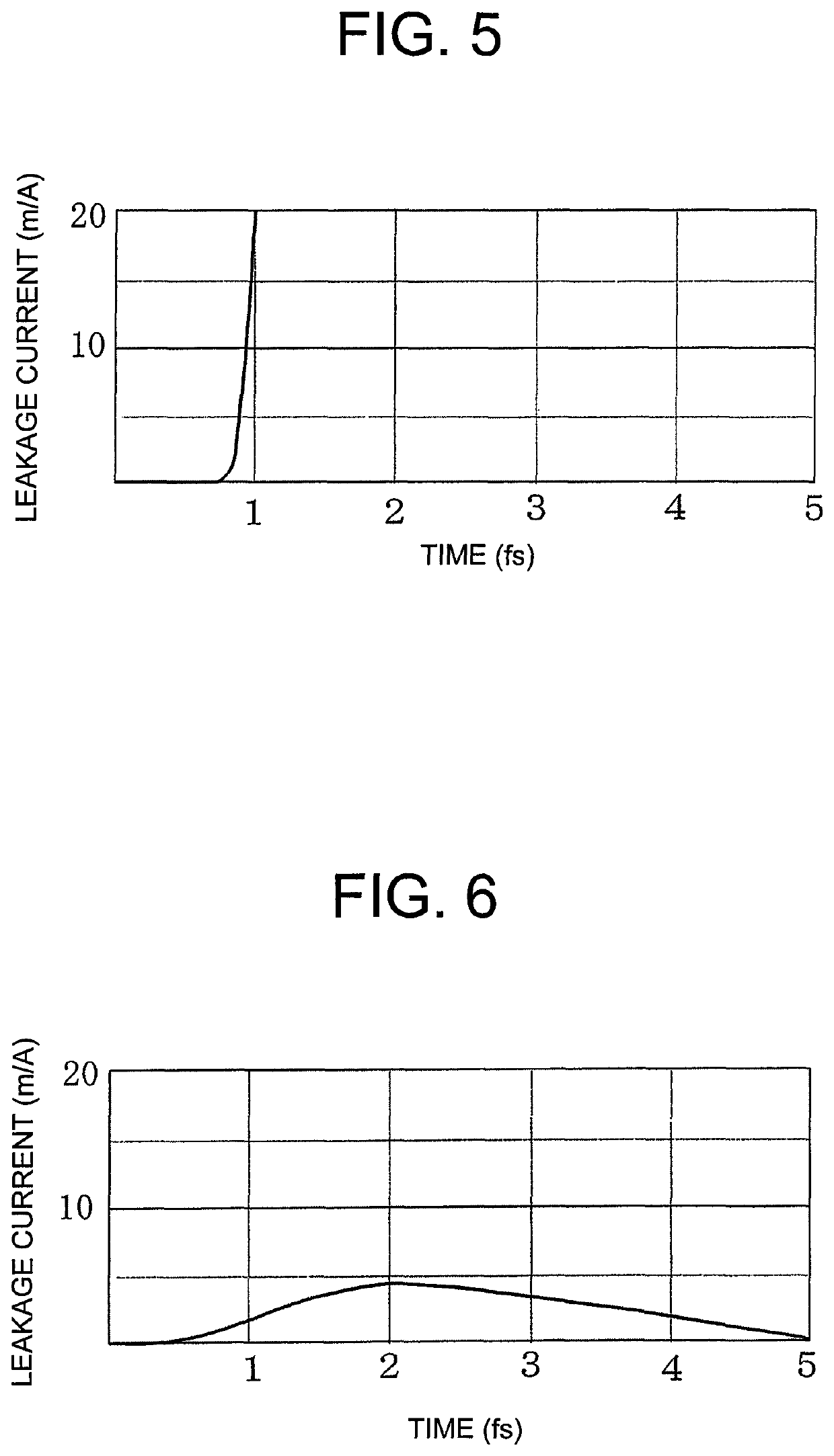
| leakage current | aaaaa | aaaaa |
| length | aaaaa | aaaaa |
| DC voltage | aaaaa | aaaaa |
Abstract
Description
Claims
Application Information