Surface treatment system for PCB manufacturing

A surface treatment, PCB board technology, applied in the field of PCB board manufacturing, can solve the problems of incapable of layered washing on the surface of the PCB board, low surface cleanliness of the PCB board, etc., and achieve the effect of reducing the area

Inactive Publication Date: 2022-04-29
无锡牛斗时空科技有限公司
View PDF0 Cites 0 Cited by
  • Summary
  • Abstract
  • Description
  • Claims
  • Application Information

AI Technical Summary

Problems solved by technology

[0003] At present, the existing surface treatment system for PCB board manufacturing has the following disadvantages: it can only perform simple immersion cleaning on the PCB board, so it cannot perform hierarchical washing on the surface of the PCB board, which makes the surface cleanliness of the PCB board relatively low Therefore, it is urgent to design a surface treatment system for PCB board manufacturing to solve the above problems

Method used


Image

  • Surface treatment system for PCB manufacturing
  • Surface treatment system for PCB manufacturing
  • Surface treatment system for PCB manufacturing

Examples


Embodiment Construction

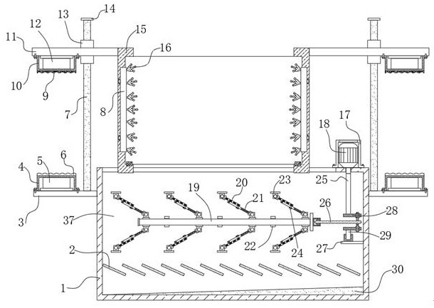
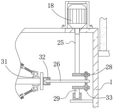
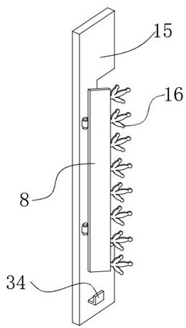
[0025] The technical solution of this patent will be further described in detail below in conjunction with specific embodiments.

[0026] Embodiments of the present patent are described in detail below, examples of which are shown in the drawings, wherein the same or similar reference numerals designate the same or similar elements or elements having the same or similar functions throughout. The embodiments described below by referring to the figures are exemplary, and are only used to explain the patent, and should not be construed as limiting the patent.

[0027] In the description of this patent, it is to be understood that the terms "center", "upper", "lower", "front", "rear", "left", "right", "vertical", "horizontal", The orientation or positional relationship indicated by "top", "bottom", "inner", "outer", etc. is based on the orientation or positional relationship shown in the drawings, and is only for the convenience of describing this patent and simplifying the descri...


PUM


Abstract

A surface treatment system for PCB manufacturing disclosed by the present invention comprises a treatment box, the top of the treatment box is provided with a rectangular immersion hole, the inner walls of the two sides of the treatment box are fixedly connected with a plurality of isolation plates, the two sides of each isolation plate are both provided with a surge mechanism, the outer walls of the two sides of the treatment box are both provided with a lifting mechanism, each surge mechanism comprises a cross rod, and the cross rod is fixedly connected with the immersion hole. The outer wall of the transverse rod is fixedly connected with a plurality of sleeve shells, the two sides of each sleeve shell are each provided with a gushing piece mechanism, each gushing piece mechanism comprises a first gushing piece and a second gushing piece, one end of each first gushing piece is rotationally connected with the outer wall of the corresponding sleeve shell through a bearing, the outer wall of each first gushing piece is provided with two strip-shaped sliding holes, and T-shaped sliding blocks are inserted into the sliding holes. According to the surface treatment system for manufacturing the PCBs, when the surfaces of the PCBs are cleaned, the PCBs can be subjected to batch treatment, and the surfaces of the PCBs can be subjected to surge type washing, so that the cleanliness is improved.

Description

technical field [0001] The invention relates to the technical field of PCB board manufacturing, in particular to a surface treatment system for PCB board manufacturing. Background technique [0002] The PCB board is an important electronic component, a support for electronic components, and a carrier for electrical connections of electronic components. Because it is made using electronic printing, it is called a "printed" circuit board. In the process of PCB board reproduction, it is necessary to clean the surface of the PCB board. [0003] At present, the existing surface treatment system for PCB board manufacturing has the following disadvantages: it can only perform simple immersion cleaning on the PCB board, so it cannot perform hierarchical washing on the surface of the PCB board, which makes the surface cleanliness of the PCB board relatively low Therefore, there is an urgent need to design a surface treatment system for PCB board manufacturing to solve the above pro...

Claims


Application Information

Patent Timeline
Patent Type & Authority Applications(China)
IPC IPC(8): H05K3/26
CPCH05K3/26
Inventor 段顺利王景荣
Owner 无锡牛斗时空科技有限公司
Why Eureka
Try Eureka