
Manufacturing method of semiconductor device

A manufacturing method and semiconductor technology, applied in semiconductor/solid-state device manufacturing, electrical components, circuits, etc., can solve the problems of difficult control of the depth of the first hole structure and side wall shape, poor stability of the hole carving process, etc., to improve the process Stability, good shape, and the effect of reducing dosage requirements

Active Publication Date: 2022-08-02
HUBEI YANGTZE PILOT-LINE SERVICES CO LTD
View PDF4 Cites 0 Cited by
  • Summary
  • Abstract
  • Description
  • Claims
  • Application Information

AI Technical Summary

Problems solved by technology

[0003] The hole etching process currently only etches a hole structure with one depth on the wafer surface. If it involves etching a hole structure with two depths or more than two depths, for example, when etching to form the second hole structure, the formed The depth and sidewall morphology of the first hole structure (different from the second hole structure) is difficult to control, resulting in poor stability of the hole carving process

Method used


Image

  • Manufacturing method of semiconductor device
  • Manufacturing method of semiconductor device
  • Manufacturing method of semiconductor device

Examples


Embodiment Construction

[0069] The technical solutions of the present disclosure will be further elaborated below with reference to the accompanying drawings and embodiments. While exemplary implementations of the present disclosure are shown in the drawings, it should be understood that the present disclosure may be embodied in various forms and should not be limited by the embodiments set forth herein. Rather, these embodiments are provided so that the present disclosure will be more thoroughly understood, and will fully convey the scope of the present disclosure to those skilled in the art.

[0070] The present disclosure is described in more detail by way of example in the following paragraphs with reference to the accompanying drawings. The advantages and features of the present disclosure will become apparent from the following description and claims. It should be noted that the accompanying drawings are all in a very simplified form and in inaccurate scales, and are only used to facilitate an...


PUM


Abstract

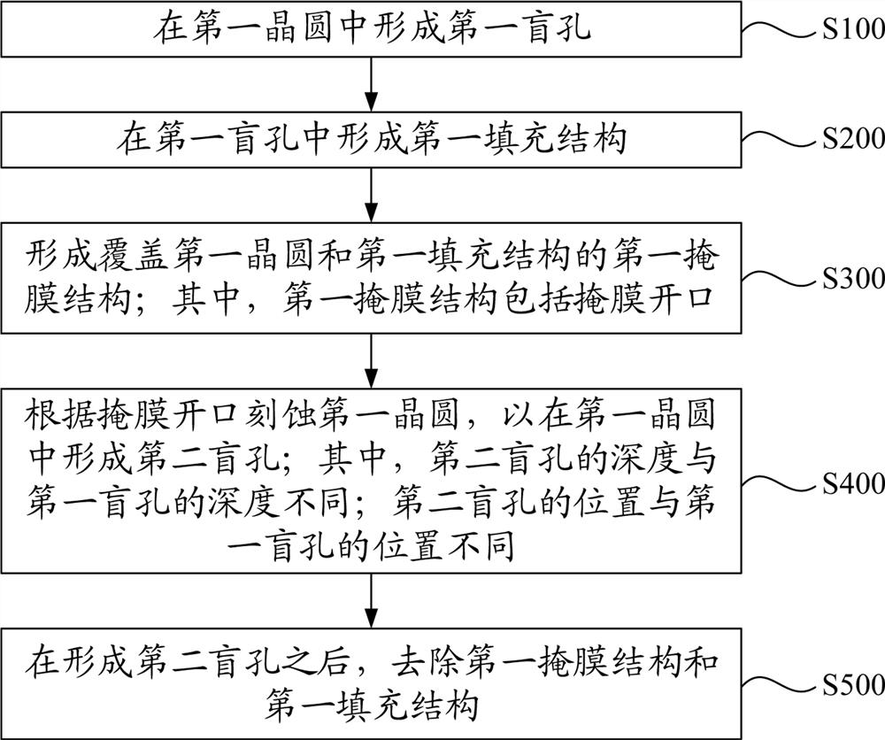
An embodiment of the present disclosure discloses a method for fabricating a semiconductor device, including: forming a first blind hole in a first wafer; forming a first filling structure in the first blind hole; forming a cover covering the first wafer and a first mask structure of the first filling structure; wherein, the first mask structure includes a mask opening; the first wafer is etched according to the mask opening, to A second blind hole is formed in the circle; wherein, the depth of the second blind hole is different from the depth of the first blind hole; the position of the second blind hole is different from the position of the first blind hole; After the second blind via, the first mask structure and the first filling structure are removed.

Description

technical field [0001] The embodiments of the present disclosure relate to, but are not limited to, the field of semiconductor manufacturing, and in particular, relate to a method for fabricating a semiconductor device. Background technique [0002] During the fabrication of semiconductor devices, hole structures (including through holes and / or blind holes) may be formed in the wafer through a hole engraving process. [0003] The hole etching process currently only etches a hole structure with one depth on the wafer surface. If it involves etching hole structures with two or more depths, for example, when etching to form a second hole structure, the already formed hole structure is etched. The depth and sidewall profile of the first hole structure (with a depth different from that of the second hole structure) are difficult to control, resulting in poor stability of the hole engraving process. SUMMARY OF THE INVENTION [0004] Embodiments of the present disclosure provide...

Claims


Application Information

Patent Timeline
Patent Type & Authority Patents(China)
IPC IPC(8): H01L21/308H01L21/768
CPCH01L21/3086H01L21/76898
Inventor 汪松王逸群程曲刘天建
Owner HUBEI YANGTZE PILOT-LINE SERVICES CO LTD
Learn More