Semiconductor module
A technology for semiconductors and shells, which is applied in the direction of semiconductor devices, semiconductor/solid-state device manufacturing, semiconductor/solid-state device components, etc. It can solve the problems of miniaturization of semiconductor modules, reduce the allowable current value, and increase the electrode width. Achieve the effects of shortening the electrode path, reducing inductance, and suppressing surge voltage
- Summary
- Abstract
- Description
- Claims
- Application Information
AI Technical Summary
Problems solved by technology
Method used
Image

Examples
Embodiment approach 1
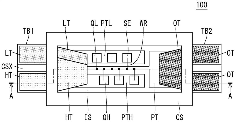
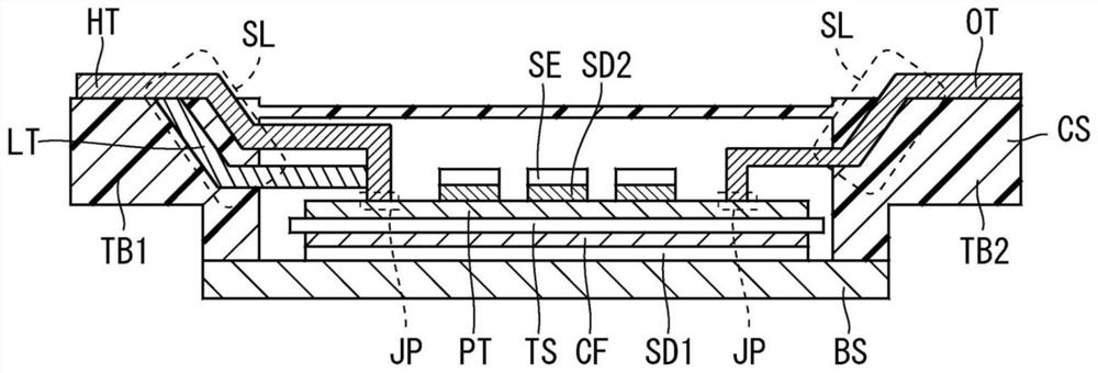
[0023] figure 1 It is a top view which shows the structure of the semiconductor module 100 of Embodiment 1, and the upper surface of the resin case CS is abbreviate|omitted in order to clarify an internal structure. in addition, figure 2 is a cross-sectional view showing the structure of the semiconductor module 100, and is figure 1 Sagittal section at line A-A in .
[0024] like figure 1 and figure 2 As shown, in the semiconductor module 100 , the upper surface of the base plate BS functioning as a heat dissipation plate and the conductor film CF on the lower surface of the insulating substrate IS are bonded via a bonding material SD1 such as solder. A circuit pattern PT is provided on the upper surface of the insulating substrate IS, and a plurality of semiconductor elements SE such as transistor chips and diode chips for power are bonded to the circuit pattern PT via a bonding material SD2 such as solder.
[0025] The insulating substrate IS is made of resin or ceram...
Embodiment approach 2
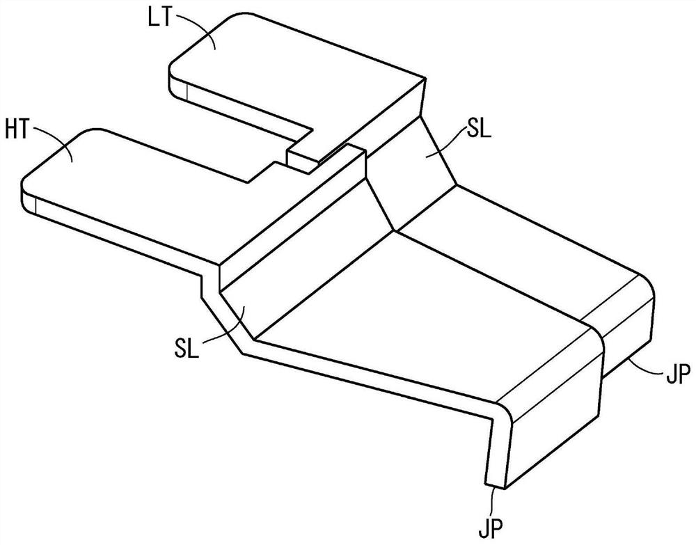
[0046] In the semiconductor module 100 of the first embodiment described above, the high-potential electrode HT, the low-potential electrode LT, and the output electrode OT each have the inclined portion SL at one location, but the inclined portion may be Each electrode is provided at a plurality of locations.
[0047] Figure 9 is a cross-sectional view showing the structure of the semiconductor module 200 according to the second embodiment, which is the same as the figure 1 The sagittal section at line A-A in the equivalent figure. Furthermore, in Figure 9 in, right and use figure 1 and figure 2 The same structures of the semiconductor modules 100 described above are marked with the same reference numerals, and repeated descriptions are omitted.
[0048] like Figure 9 As shown, one end of the high potential electrode HT and the low potential electrode LT of the semiconductor module 200 is exposed at the upper surface of the terminal block TB1 protruding from the sid...
Embodiment approach 3
[0053] Figure 10 and Figure 11 They are a plan view and a cross-sectional view, respectively, for explaining the manufacturing method of the semiconductor module 300 according to the third embodiment. Furthermore, in Figure 10 and Figure 11 in, right and use figure 1 and figure 2 The same structures of the semiconductor modules 100 described above are marked with the same reference numerals, and repeated descriptions are omitted.
[0054] like Figure 10 and Figure 11 As described above, the semiconductor module 300 has the case CS completed by forming the side walls of the case CS in which the high-potential electrodes HT and the low-potential electrodes LT are housed independently of other parts of the case CS, The separate side wall CSX is joined to the other parts of the casing CS by adhesive or the like. Therefore, there is a seam between the side wall CSX and the other parts.
[0055] The closer the inter-electrode distance between the high-potential elect...
PUM
 Abstract
Description
Claims
Application Information
 - R&D Engineer
- R&D Manager
- IP Professional
- Industry Leading Data Capabilities
- Powerful AI technology
- Patent DNA Extraction
Browse by: Latest US Patents, China's latest patents, Technical Efficacy Thesaurus, Application Domain, Technology Topic.
© 2024 PatSnap. All rights reserved.Legal|Privacy policy|Modern Slavery Act Transparency Statement|Sitemap