Punch-through gate co-implant species for controlling dopant distribution in transistors
A dopant and transistor technology, applied in the direction of transistors, semiconductor devices, electrical solid state devices, etc., can solve the problem of reducing the density of bare chip devices
- Summary
- Abstract
- Description
- Claims
- Application Information
AI Technical Summary
Problems solved by technology
Method used
Image

Examples
Embodiment Construction
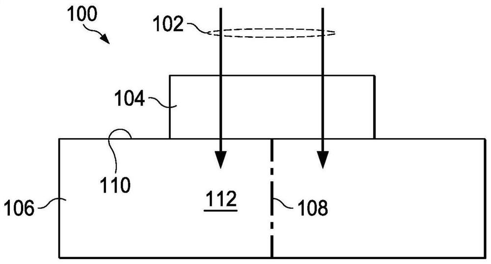
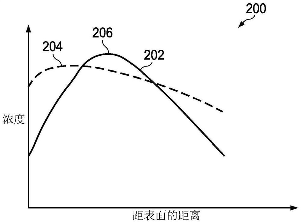
[0020] Example embodiments relate to transistors and integrated circuits including transistors that exhibit improved mismatch. For example, one or more metal-oxide-semiconductor (MOS) transistors include dopants and through-gate co-plants in the channel region of the substrate positioned under the gate structure between the drain and source regions into the species. The dopant species may include well dopants and channel dopants. The co-implanted species are implanted with sufficient energy to pass through the gate structure (eg, polysilicon and gate dielectric layers) and into the substrate. During fabrication, the co-implanted species control (eg, retard) the diffusion of dopant species to establish an inverse dopant profile in response to annealing. In an example, the inverse profile provides a dopant concentration that increases from the substrate surface to a location of peak concentration spaced from the substrate surface, and then decreases from the location of peak c...
PUM
| Property | Measurement | Unit |
|---|---|---|
| thickness | aaaaa | aaaaa |
| relative permittivity | aaaaa | aaaaa |
Abstract
Description
Claims
Application Information
 - R&D Engineer
- R&D Manager
- IP Professional
- Industry Leading Data Capabilities
- Powerful AI technology
- Patent DNA Extraction
Browse by: Latest US Patents, China's latest patents, Technical Efficacy Thesaurus, Application Domain, Technology Topic.
© 2024 PatSnap. All rights reserved.Legal|Privacy policy|Modern Slavery Act Transparency Statement|Sitemap