Transmitting circuit, receiving circuit, receiving and transmitting circuit and electrooptical apparatus
A signaling circuit and circuit technology, applied in the direction of logic circuit coupling device, logic circuit connection/interface arrangement, logic circuit, etc., can solve the problem of delay time increase, stray capacitance Cx can not be ignored, transparent conductor wiring spacing is narrow, etc. question
- Summary
- Abstract
- Description
- Claims
- Application Information
AI Technical Summary
Problems solved by technology
Method used
Image

Examples
Embodiment 1
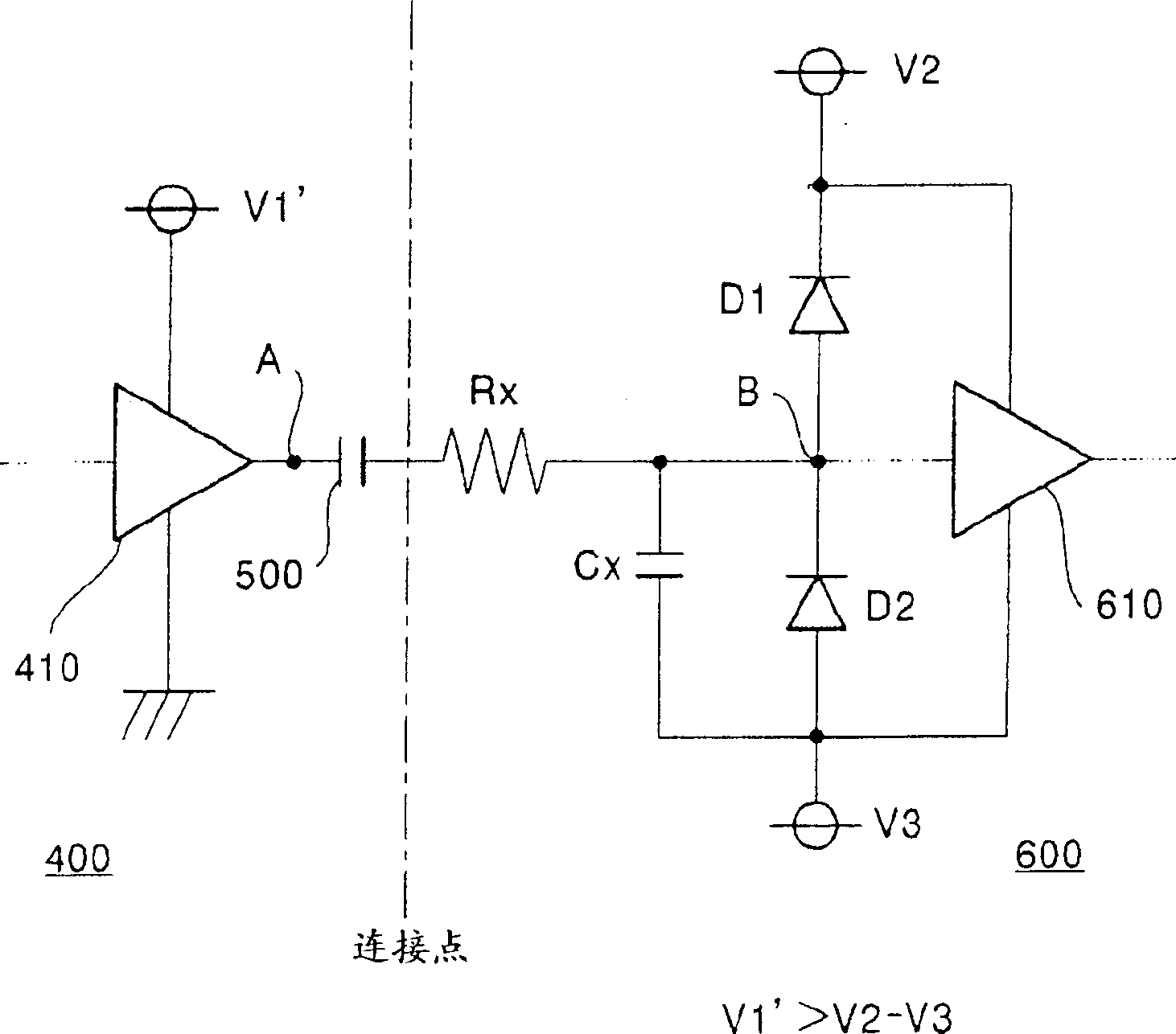
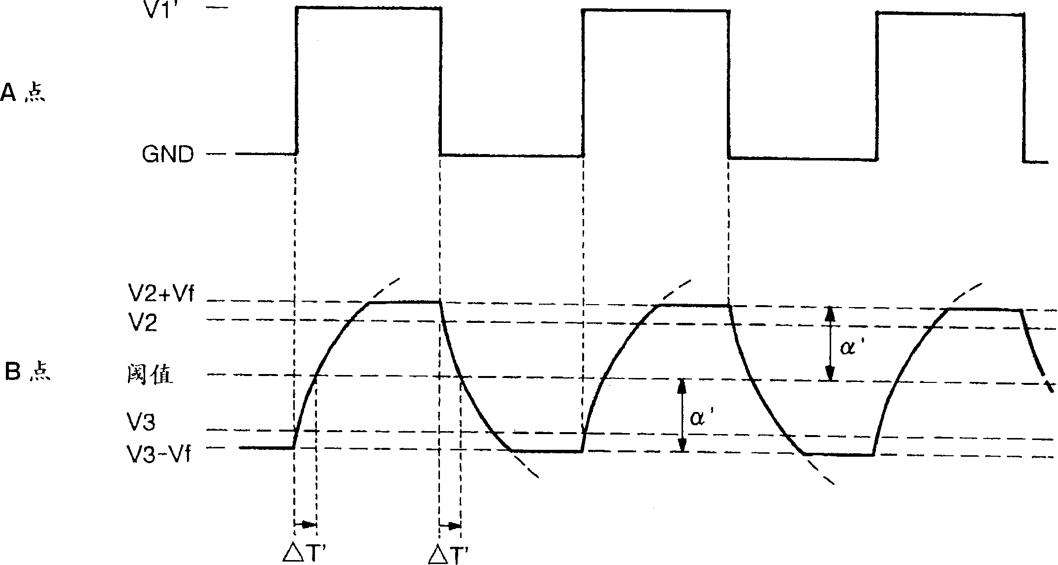
[0083] First, Embodiment 1 of the present invention will be described. figure 1 is a block diagram showing its structure. As shown in the figure, in this embodiment, in the signaling circuit 400, the power supply voltage of the buffer 410 for transmitting logic signals is increased from V1 to V1'. In this way, if figure 2 As shown, the amplitude of the logic signal at the output point A becomes "V1'-GND", which is greater than the power supply voltage of the buffer 610 that inputs the logic signal in the receiving circuit 600. At this time, assuming that the forward voltage drop of the protection diodes D1 and D2 is Vf, the amplitude of the logic signal at the input point B is amplified from "V2+Vf" which is the clipping level of the protection diodes D1 and D2 to "V3- Vf".
[0084] Therefore, in the buffer 610 receiving the logic signal in the receiver circuit 600, the delay time of the output signal is ΔT', which is shorter than the conventional delay time ΔT even if th...
Embodiment 2
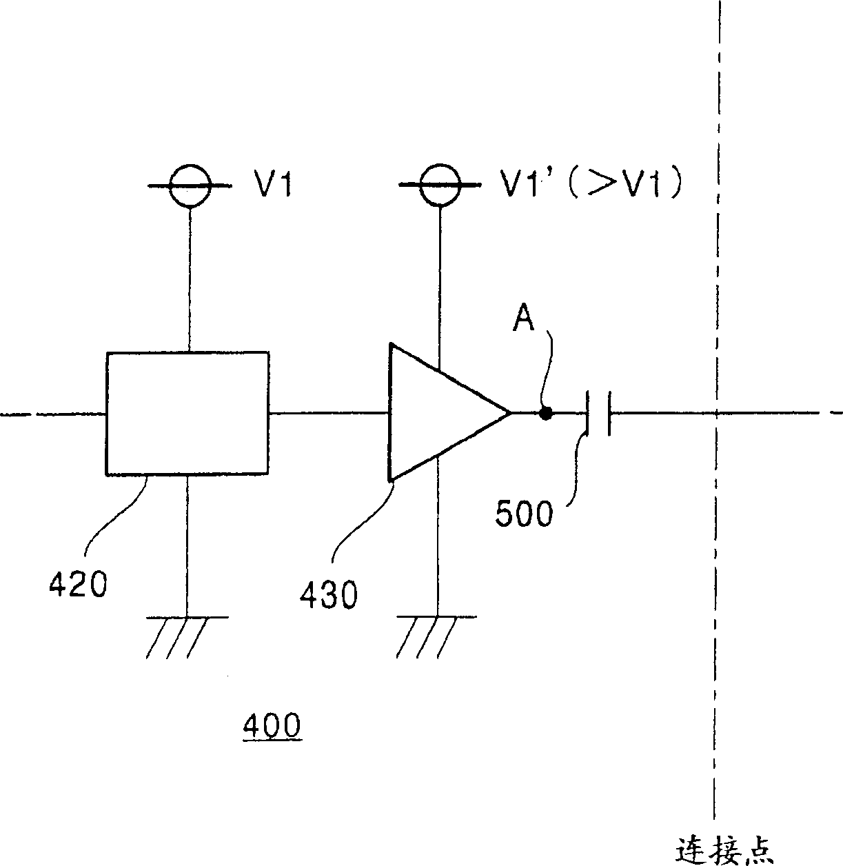
[0086] Next, Embodiment 2 of the present invention will be described. image 3 is a block diagram showing its structure. In the figure, the processing circuit 420 is a circuit that performs logic processing in the transmitting circuit 400, and uses the previous "V1-GND" as a power supply voltage. On the other hand, the buffer 430 amplifies the amplitude of the logic signal of the processing circuit 420 using the higher "V1'-GND" as a power supply voltage. That is, the buffer 430 functions as a level shifter.
[0087] Here, the input-output characteristics of the buffer 430 are, for example, Figure 4 properties shown. That is, the buffer 430 buffers the input logic signal with (V1) / 2 as the threshold. Additionally, such a buffer 430, such as Figure 5 As shown, it is a configuration in which inverters INV1 and INV2 are connected in two stages. Here, each of the inverters INV1 and INV2 has a structure in which a P-channel transistor and an N-channel transistor are respect...
Embodiment 3
[0091] First, Embodiment 3 of the present invention will be described. Figure 6 is a block diagram showing the structure. As shown, the supply voltage V1' of the buffer 430 is not additionally generated, but is generated from a previous supply voltage V1 in the manner described below.
[0092] First, a control signal CRT with a duty ratio of approximately 50%, a voltage V1 at a high level, and a ground potential GND at a low level is supplied to point F. Here, point F is connected to point G through a capacitor Ca. In addition, this G point is connected to the supply line of the power supply voltage V1 through a diode D3. In addition, point D is connected to point H through a diode D4 , and the voltage at point H is supplied as the positive side power supply voltage of buffer 420 . A capacitor Cb for maintaining voltage is inserted between the H point and the ground potential GND.
[0093] In such a configuration, when the control signal CRT is at a low level, forward cur...
PUM
 Abstract
Description
Claims
Application Information
 - R&D Engineer
- R&D Manager
- IP Professional
- Industry Leading Data Capabilities
- Powerful AI technology
- Patent DNA Extraction
Browse by: Latest US Patents, China's latest patents, Technical Efficacy Thesaurus, Application Domain, Technology Topic.
© 2024 PatSnap. All rights reserved.Legal|Privacy policy|Modern Slavery Act Transparency Statement|Sitemap