
Eureka
For R&D, Eureka makes reading and utilizing patents & technical documents easy.
Eureka AIR
Designed for self-driven R&D workflows. Generate viable solutions, solve complex R&D challenges, empower your innovation with AI.

Eureka Materials
Designed for material experts only. Revolutionize your material R&D, from search, analyze, to developing new materials.

TechResearch
Generate reliable direction feasibility study reports for your R&D in just a few steps.

TechSeek
Discover and master advanced knowledge NOW. Basics, ideas, possibilities, all at once.

TechMind
As an expert in R&D Theories, TechMind can generates customized viable solutions instantly.

TechRisk
Analyze your overall solution with one click, know your potential R&D risks in advance.

TechMonitor
Get weekly tech updates, stay abreast of the latest tech innovations and key insights.
Phosphor ink coating device, plasma display panel, and method of manufacturing the plasma display panel
A fluorescent ink and coating device technology, applied in the manufacture of discharge tubes/lamps, devices for coating liquid on the surface, fluorescent layers, etc., can solve the problems of not being able to display full color, color mixing, etc.
- Summary
- Abstract
- Description
- Claims
- Application Information
AI Technical Summary
Problems solved by technology
Method used
Image

Examples
no. 1 example
[0035] A first embodiment of the fluorescent ink application apparatus of the present invention will be described below with reference to the accompanying drawings.
[0036] [Structure of PDP]
[0037] First, the structure of the PDP 100 produced by applying fluorescent ink by a fluorescent ink application device will be described.
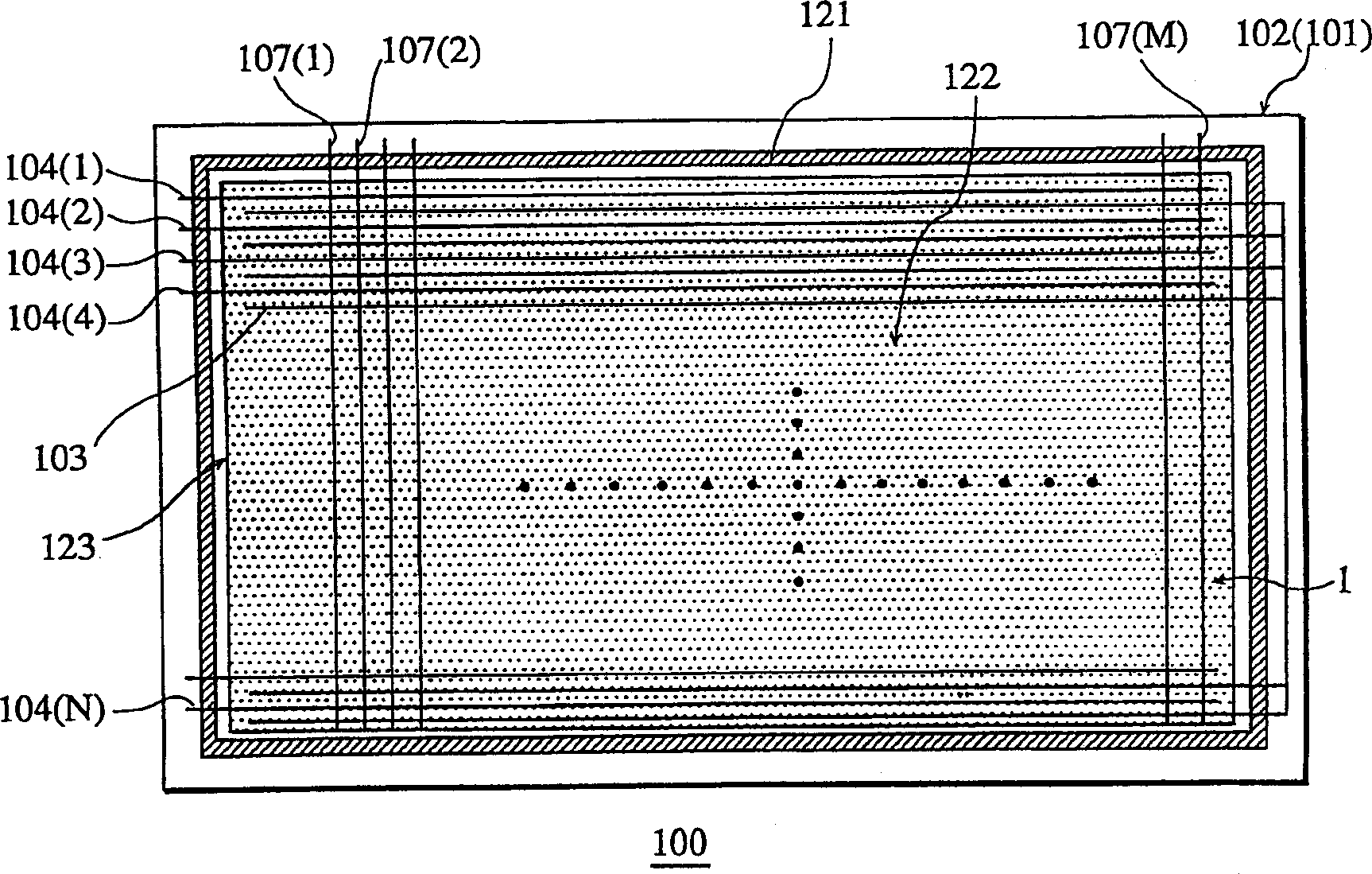
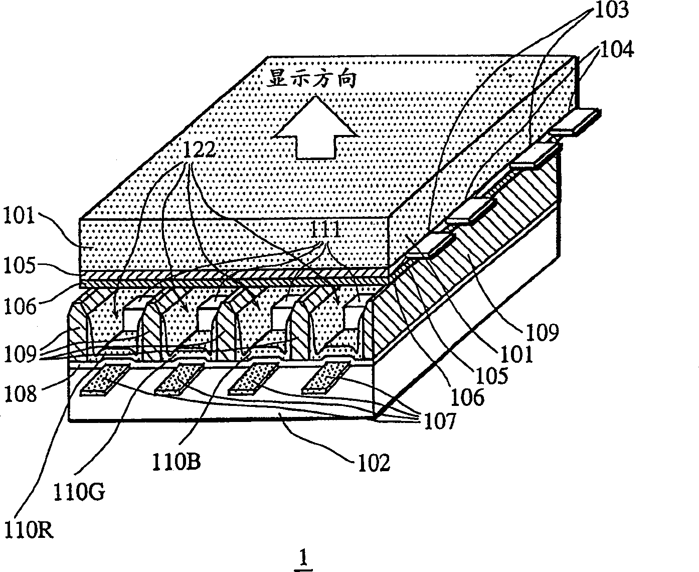
[0038] figure 1 is a schematic plan view of the PDP 100 with the front glass substrate removed, figure 2 It is a partially cutaway perspective view showing the image display area 123 of the PDP 100 . In addition, in figure 1In the figure, the number of display electrodes 103, display scan electrodes 104, address electrodes 107, etc. are partially omitted for easy understanding. Referring to these two figures, the structure of PDP 100 will be described.
[0039] like figure 1 As shown, the PDP 100 consists of a front glass substrate 101 (not shown in the figure), a rear glass substrate 102, N display electrodes 103, and N display scanning...
no. 2 example
[0127] Next, a second embodiment of the fluorescent ink application apparatus according to the present invention will be described. Please note that the fluorescent ink application device in this second embodiment, except Figure 5 outside the nozzle member 750 of the marked first embodiment, with Figure 4 , Figure 5 Basically the same as shown. Therefore, the different parts will be explained below as a center.
[0128] Figure 8 It is an exploded perspective view showing the structure of the nozzle member 750 of the fluorescent ink ejection device of the second embodiment.
[0129] As shown, the nozzle member 780 includes a cap portion 781 and a spout portion 782 which are positioned in alignment with each other and hermetically secured together. The cover part 781 is made of a flat stainless steel material, and its central part is provided with an inlet 783 for introducing fluorescent ink into the ejection part 782 .
[0130] The ejection part 782 includes: an ink s...
PUM
 Abstract
Description
Claims
Application Information
 - R&D Engineer
- R&D Manager
- IP Professional
- Industry Leading Data Capabilities
- Powerful AI technology
- Patent DNA Extraction
Browse by: Latest US Patents, China's latest patents, Technical Efficacy Thesaurus, Application Domain, Technology Topic, Popular Technical Reports.
© 2024 PatSnap. All rights reserved.Legal|Privacy policy|Modern Slavery Act Transparency Statement|Sitemap|About US| Contact US: help@patsnap.com