Laminated dielectric filter
A filter and stacking technology, applied in waveguide devices, waveguides, circuits, etc., can solve problems such as unfavorable filters
- Summary
- Abstract
- Description
- Claims
- Application Information
AI Technical Summary
Problems solved by technology
Method used
Image
Examples
Embodiment Construction
[0082] Refer below Figure 1-29 Several illustrative embodiments of a laminated type dielectric filter according to the present invention are explained. In the following embodiments, the case where the input terminal is unbalanced and the output terminal is balanced is roughly explained. The present invention is also applicable to the case opposite to the above.
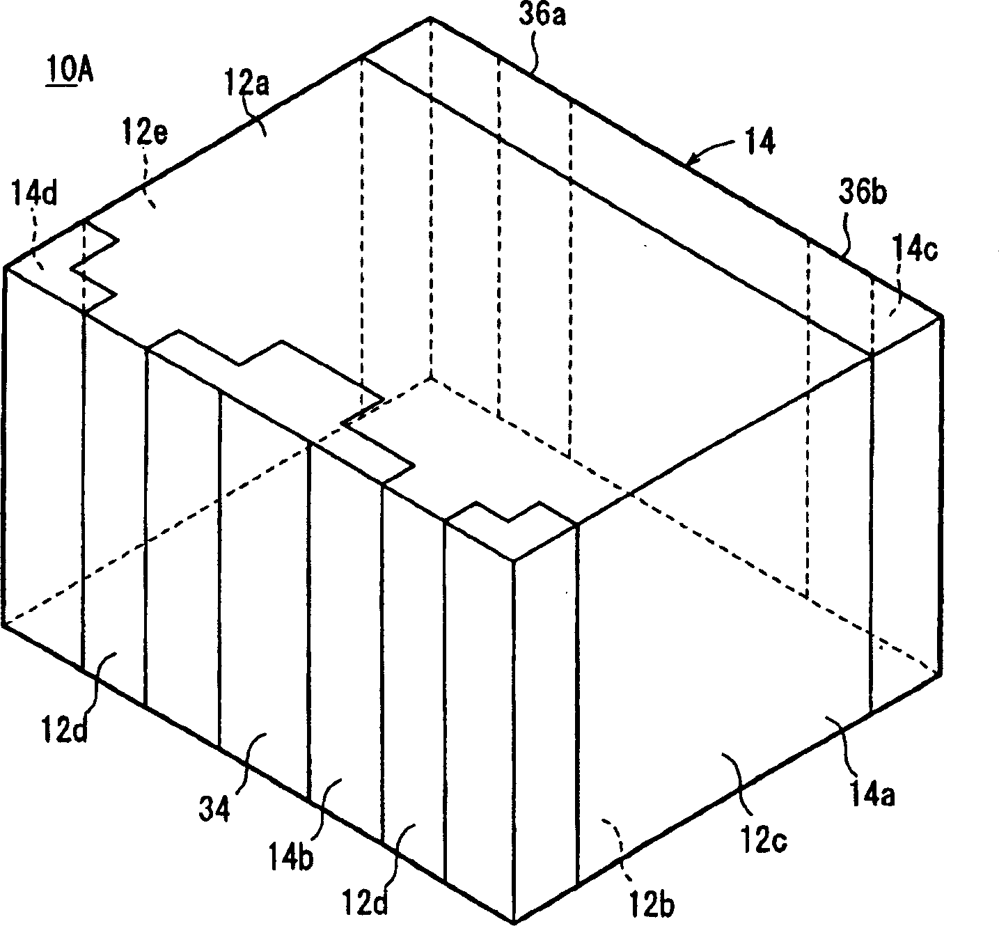
[0083] Such as figure 1 As shown, the laminated dielectric filter 10A of the first embodiment has a dielectric substrate 14 . The dielectric substrate 14 includes a plurality of dielectric layers (S1-S10, see figure 2 ). Ground electrodes 12a, 12b are formed on both main surfaces of the dielectric substrate 14 (the first main surface of the first dielectric layer S1 and the first main surface of the tenth dielectric layer S10).
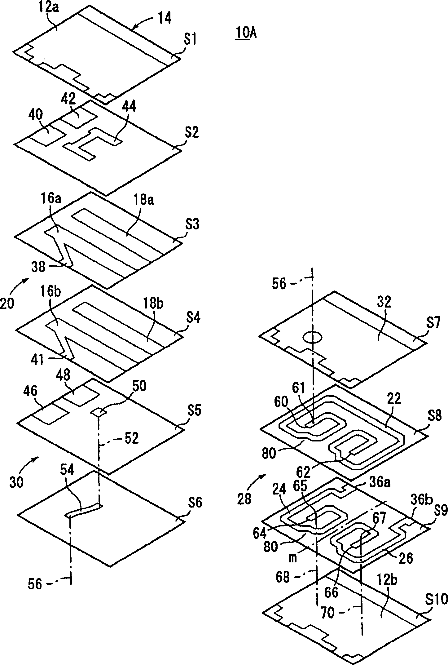
[0084] Such as figure 2 As shown, a filter element 20 , an unbalanced-balanced conversion element (transition element 28 ), and a connection element 30 are disposed within the diele...
PUM
 Abstract
Description
Claims
Application Information


