Image display device and display drive method

A technology of image display and display drive, applied to static indicators, instruments, etc., can solve problems such as increased leakage current, increased source-drain voltage VDS1, and decreased pixel display density

Inactive Publication Date: 2003-05-28
SHARP KK
View PDF0 Cites 22 Cited by
  • Summary
  • Abstract
  • Description
  • Claims
  • Application Information

AI Technical Summary

Problems solved by technology

On the contrary, on the pixel PIX1 that keeps the positive polarity charge, the above-mentioned source-drain voltage VDS1 becomes larger, and the leakage current also becomes larger, and the display density of the pixel having the positive polarity charge decreases during the non-scanning period (normal later occasions) the problem

Method used


Image

  • Image display device and display drive method
  • Image display device and display drive method
  • Image display device and display drive method

Examples


Embodiment Construction

[0034] An embodiment of the present invention will be described below with reference to the accompanying drawings.

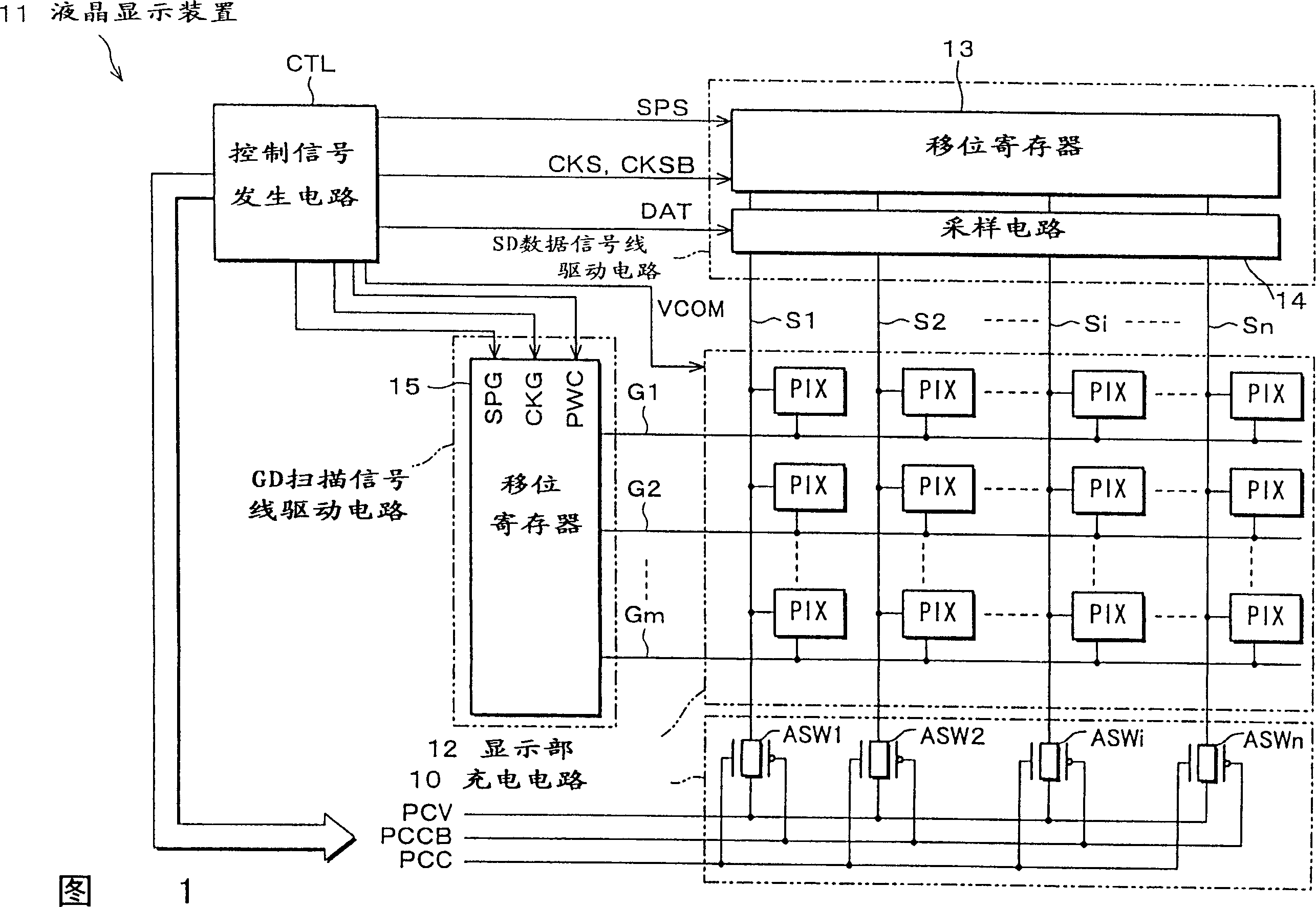
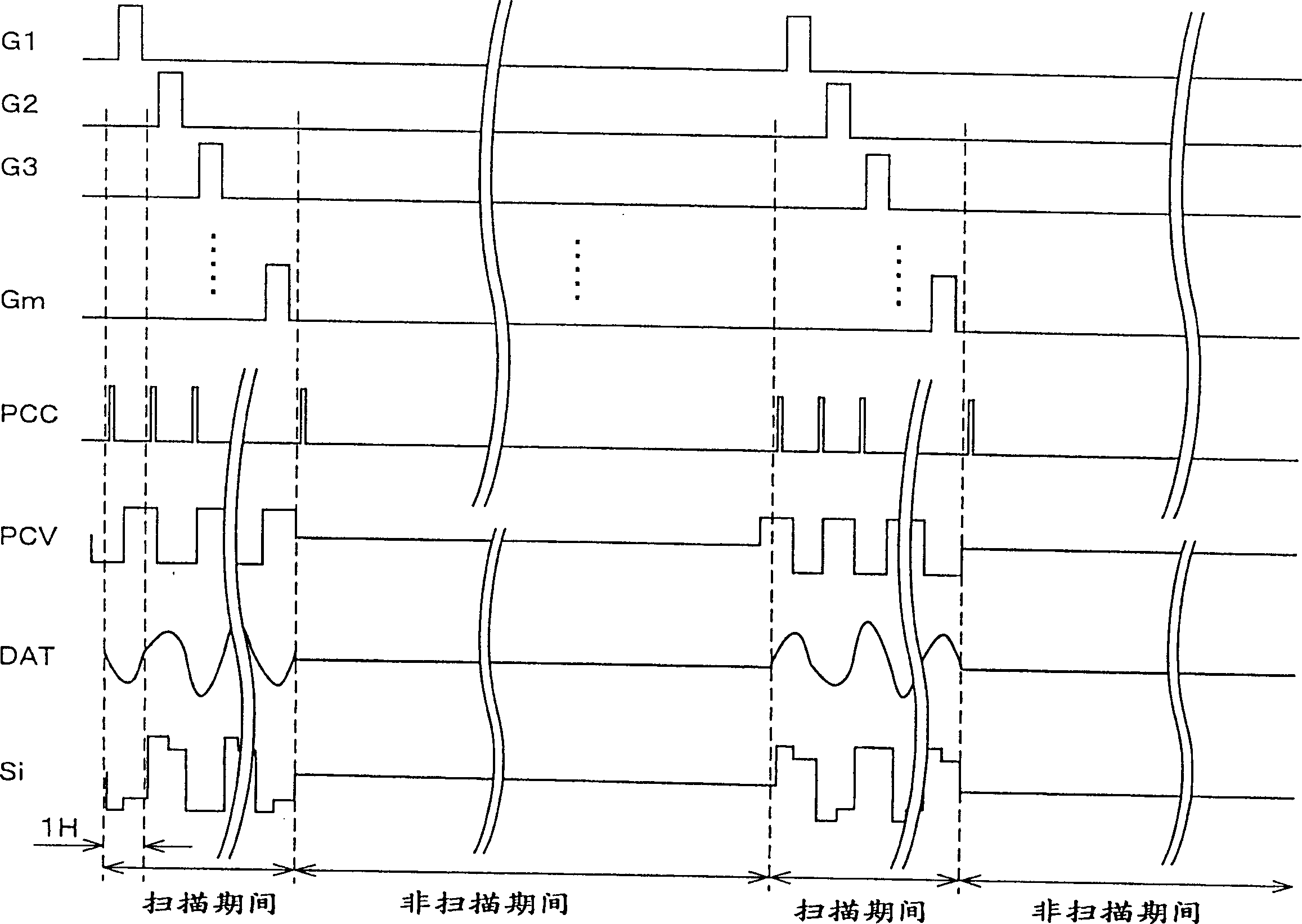
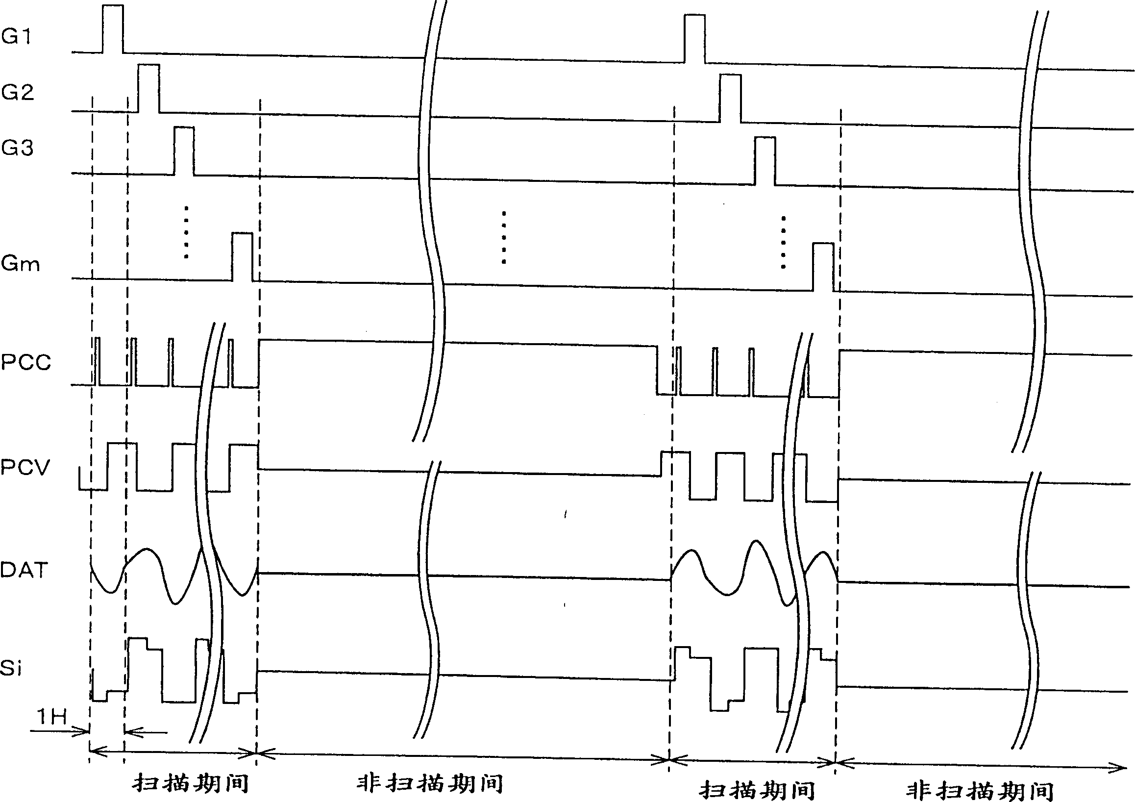
[0035] FIG. 1 is a block diagram showing an electrical configuration of a liquid crystal display device 11 as an image display device according to an embodiment of the present invention. The liquid crystal display device 11 is an active matrix liquid crystal display device, and generally includes a display unit 12, a scanning signal line driving circuit GD, a data signal line driving circuit SD, a charging circuit 10, and a control signal generating circuit CTL. The above-mentioned data signal line driving circuit SD is composed of a shift register 13 and a sampling circuit 14 , and the scanning signal line driving circuit GD is composed of a shift register 15 . The data signal line driver circuit SD and the scanning signal line driver circuit GD have the same configurations as the data signal line driver circuit Sd and the scanning signal line driver circuit gd...


PUM


Abstract

The output of a data signal line driving circuit becomes high-impedance by a charge circuit during a non-scanning period and that a potential of a data signal line S during a scanning period is charged to a substantially intermediate potential of a data signal at a corresponding frame. Thus, extremely large dispersion does not occur in a potential of each pixel capacitor with respect to a potential of the data signal line S, so that it is possible to restrict dispersion of a leak current flowing via an active element of each pixel. Thus, potential variation of a pixel PIX is reduced, so that it is possible to improve display quality during a non-scanning period. That is, in an active-matrix-type liquid crystal display, when a frame frequency is reduced by setting the non-scanning period to be sufficiently larger than a scanning period while a standby image is being displayed so as to realize low power consumption, the display quality is improved.

Description

technical field [0001] The present invention relates to an electro-optic element formed on an area divided by a plurality of scanning signal lines and data signal lines intersecting each other, and an active element and a pixel capacitor formed in pairs on it which is most suitable for implementation as a liquid crystal display device An active matrix image display device and a driving method thereof. In particular, it relates to an image display device and a display driving method with a low frame rate and low power consumption, in which the scan cycle is set to be sufficiently long relative to the scan cycle when the screen is in standby. Background technique [0002] Figure 8 It is a block diagram showing a typical prior art image display device of an active matrix type, and an electrical configuration constituting a liquid crystal display device 1 . The liquid crystal display device 1 roughly includes a display unit 2, a scanning signal line driving circuit gd, a data ...

Claims


Application Information

Patent Timeline
Patent Type & Authority Applications(China)
IPC IPC(8): G02F1/133G09G3/20G09G3/36
CPCG09G3/3648G09G3/3688G09G2330/021G09G2310/0248G09G3/36
Inventor 鹫尾一海濑泰佳前田和宏久保田靖
Owner SHARP KK
Why Eureka
Try Eureka