Electric absorption modulation distribution feedback laser of mixed wave guide structure and producing method

An electro-absorption modulator and electro-absorption modulation technology, applied in semiconductor lasers, lasers, laser parts, etc., can solve the problems of low laser light output efficiency, affecting laser life, and difficult to reach laser thresholds.

Inactive Publication Date: 2003-06-25
INST OF SEMICONDUCTORS - CHINESE ACAD OF SCI
View PDF1 Cites 13 Cited by
  • Summary
  • Abstract
  • Description
  • Claims
  • Application Information

AI Technical Summary

Problems solved by technology

Using the buried strip structure, in order to achieve the required modulation rate, semi-insulating InP must be used to bury it, and iron doping will bring a series of problems, such as: interdiffusion of iron and zinc affects the

Method used


Image

  • Electric absorption modulation distribution feedback laser of mixed wave guide structure and producing method
  • Electric absorption modulation distribution feedback laser of mixed wave guide structure and producing method

Examples


Embodiment Construction

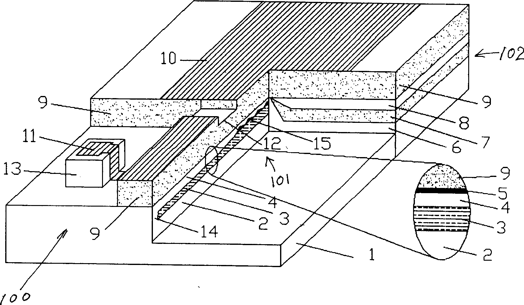
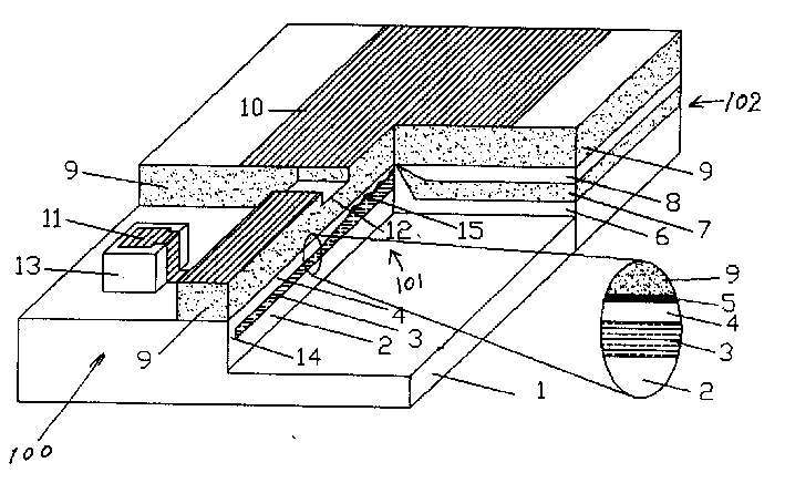
[0026] The invention combines the advantages of the buried strip structure and the ridge waveguide structure, adopts the buried strip structure in the laser part, and adopts the ridge waveguide structure in the modulator part, and makes full use of the advantages of these two structures in the laser and modulator; After the laser part is buried with a heterojunction, the threshold can be reduced and the efficiency can be improved, and there is no problem of interdiffusion of iron and zinc buried in semi-insulating InP, and the service life can be guaranteed; after the modulator part uses a ridge waveguide structure, the parasitic capacitance can be reduced , The high-speed operation of the modulator can be guaranteed; a ridge waveguide structure is used between the laser and the modulator, which is easy to achieve a high degree of isolation between the laser and the modulator, and reduces crosstalk.

[0027] An example of the present invention is as follows. like figure 1 As ...


PUM

PropertyMeasurementUnit
Lengthaaaaaaaaaa
Lengthaaaaaaaaaa
Lengthaaaaaaaaaa

Abstract

This invention relates to feed back laser of mixed waveguide structure electric adsorbing modulation distribution including: back waveguide structure electric absorbing modulator, back waveguide structure isolation zone connecting with the said electric absorbing modulator, buried heterostructure DFB isolation zone connecting with the said laser, the said absorbing modulator, isolation zone and the laser are mounted on the same substrate.

Description

technical field [0001] The invention relates to a feedback laser and a manufacturing method, in particular to a hybrid waveguide structure electro-absorption modulation distributed feedback laser and a manufacturing method, which can realize high-efficiency, low-threshold electro-absorption modulation distributed feedback laser [distributed feedback laser (DFB -LD) and electroabsorption modulator (EA modulator) monolithic integrated device, also known as EML] new structure. Background technique [0002] Electroabsorption modulated DFB lasers have become the main light source used in long-distance mainline high-speed optical communication systems. The main structures currently used are: 1) Ridge waveguide structure buried in polyimide, which was published in 1987 by Japan's KDD company Article on page 1277 of Journal of Lightwave Technology, LT-5(9), published by NTT Corporation of Japan in 1992, article on page 16 of IEEE Photonics Technology Letter, 4(1), published by Franc...

Claims


Application Information

Patent Timeline
IPC IPC(8): H01S5/00
Inventor 刘国利王圩朱洪亮
Owner INST OF SEMICONDUCTORS - CHINESE ACAD OF SCI
Why Eureka
Try Eureka