AC timing parameter controlling circuit and method for semiconductor memory equipment

A technology for storage devices and timing parameters, applied in the field of circuits, can solve problems such as reducing the performance of semiconductor storage devices

Inactive Publication Date: 2003-07-30
SAMSUNG ELECTRONICS CO LTD
View PDF0 Cites 18 Cited by
  • Summary
  • Abstract
  • Description
  • Claims
  • Application Information

AI Technical Summary

Problems solved by technology

[0006] However, when applying MRS, in case the AC timing parameters change and need to reflect their changes, the programming process of MRS must be performed separately

Method used


Image

  • AC timing parameter controlling circuit and method for semiconductor memory equipment
  • AC timing parameter controlling circuit and method for semiconductor memory equipment
  • AC timing parameter controlling circuit and method for semiconductor memory equipment

Examples


Embodiment Construction

[0043] The invention is described herein with reference to the accompanying drawings which illustrate preferred embodiments of the invention. Systematic reference numbers indicate the same parts throughout the drawings.

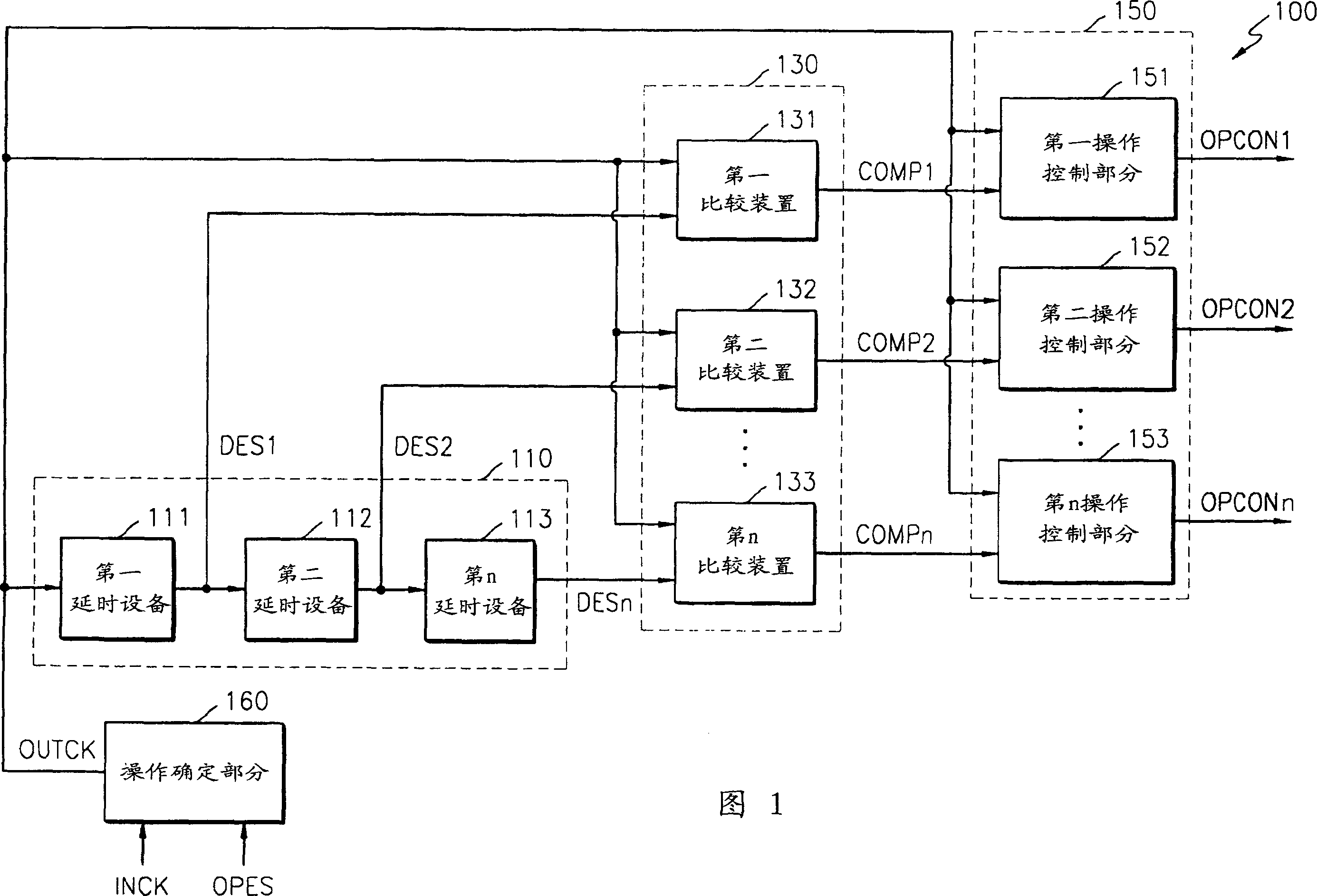
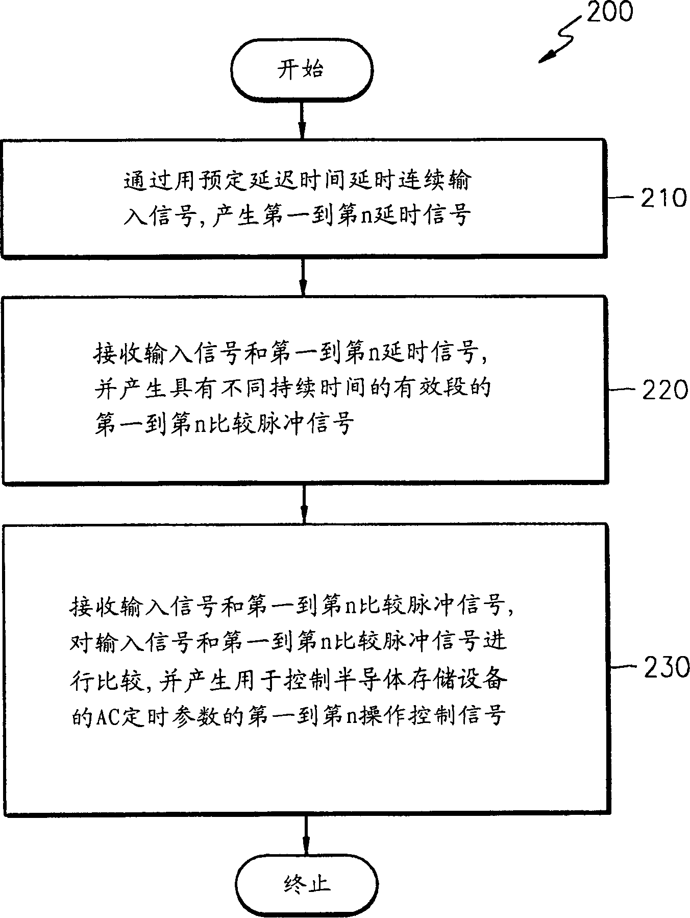
[0044] 1 is a block diagram of an AC timing parameter control circuit of a semiconductor memory device according to a first embodiment of the present invention. Referring to FIG. 1 , the AC timing parameter includes a delay time defining part 110 , a comparing part 130 and a controlling part 150 .

[0045]The delay time definition part 110 receives the continuous input signal INCK (by the optional operation determination part 160 in Fig. 1), delays the input signal INCK with a corresponding predetermined delay time, and generates the first to nth (n is a natural number) delay Timing signals DES1, DES2, . . . , DESn.

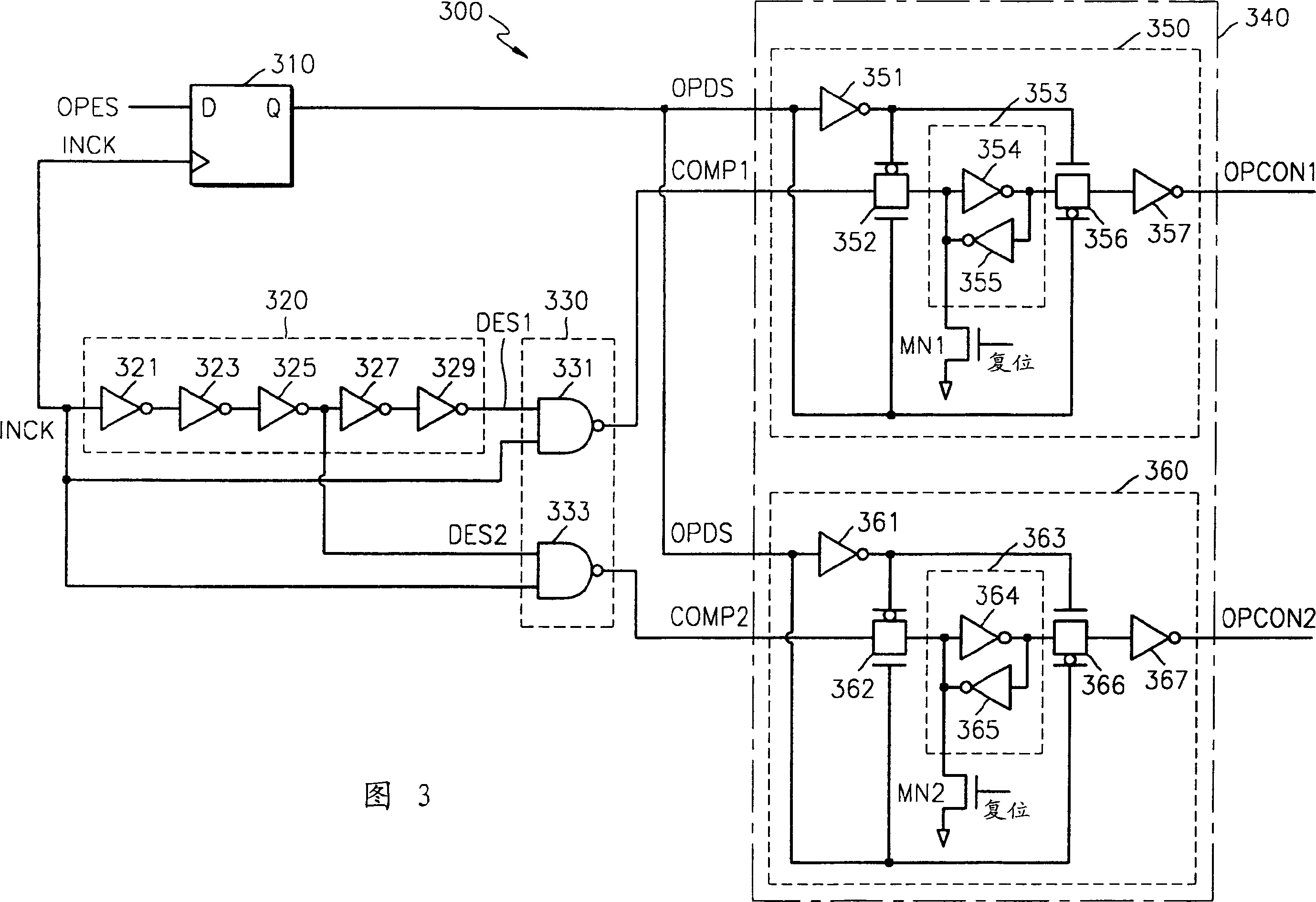
[0046] The input signal INCK is a semiconductor memory device clock signal or a command. Specifically, the delay time defining part 110 incl...


PUM


Abstract

A circuit for controlling an AC-timing parameter of a semiconductor memory device and method thereof are provided. The AC-timing parameter control circuit includes a delay-time-defining portion, a comparing portion, and a controlling portion. The control circuit compares the pulse width or period of an input signal to one or more different reference-widths pulses, with the reference width(s) set by the delay-time-defining portion and the reference pulses generated by the comparing portion. The controlling portion indicates whether the input signal width or period was less than or greater than each o the reference-width pulses. The control circuit output signals can be used to tailor the operation of the device based on a direct comparison of an AC-timing parameter to one or more reference values.

Description

technical field [0001] The present invention relates to a semiconductor storage device, and more particularly to a circuit for controlling the AC timing parameters of the semiconductor storage device and controlling the operation of the semiconductor storage device by identifying changes in the AC timing parameters. Background technique [0002] The operation timing (also called AC timing) parameter of the semiconductor storage device defines a specific operation time or a time interval between specific operations, and specifies the allowable limit of operation timing to ensure the normal operation of the semiconductor storage device. [0003] Generally, a specific value of an AC timing parameter of a semiconductor memory device is defined as a plurality of predetermined reference times or periods of a reference clock signal. The larger the allowable limit for a specific value of the AC timing parameter, the better the performance of the semiconductor memory device can be gu...

Claims


Application Information

Patent Timeline
IPC IPC(8): G11C11/407G11C7/00G11C7/10G11C7/22
CPCG11C7/222G11C7/1045G11C7/22G11C2207/2254G11C7/00
Inventor 赵正显金炳喆
Owner SAMSUNG ELECTRONICS CO LTD
Why Eureka
Try Eureka