Semiconductor equipment

A technology of semiconductors and components, applied in the field of semiconductor devices, can solve problems such as difficult clock signals

Inactive Publication Date: 2003-07-30
MITSUBISHI ELECTRIC CORP
View PDF0 Cites 3 Cited by
  • Summary
  • Abstract
  • Description
  • Claims
  • Application Information

AI Technical Summary

Problems solved by technology

[0018] However, it is not easy to generate a clock signal with consistent phase

Method used


Image

  • Semiconductor equipment
  • Semiconductor equipment
  • Semiconductor equipment

Examples


Embodiment 1

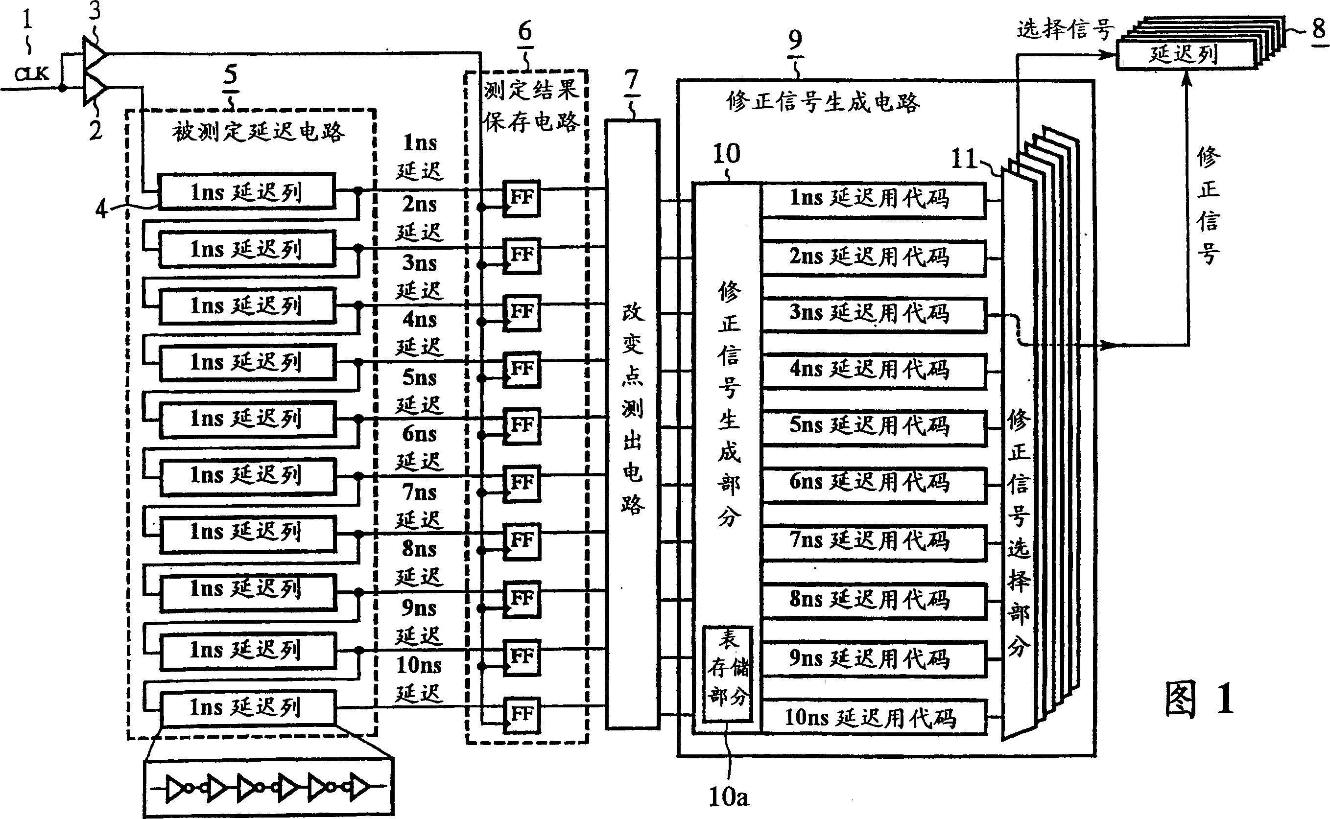
[0059] FIG. 1 is a configuration diagram of a delay adjustment circuit (semiconductor device) according to Embodiment 1 of the present invention. In the figure, 1 refers to the clock signal CLK whose period is determined, and 2 and 3 refer to the buffer units of the input clock signal CLK1.

[0060] 4 is a 1ns delay column (delay component), which is designed according to the requirement of adjusting the number of inverter chain elements to respectively achieve the 1ns set delay amount; 5 is the measured delay circuit (measured delay component), which is composed of multiple 1ns delays The columns 4 are connected in series, and after the clock signal CLK1 is input through the buffer unit 2, the phase of the clock signal CLK1 is changed by delaying the column 4 by 1 ns.

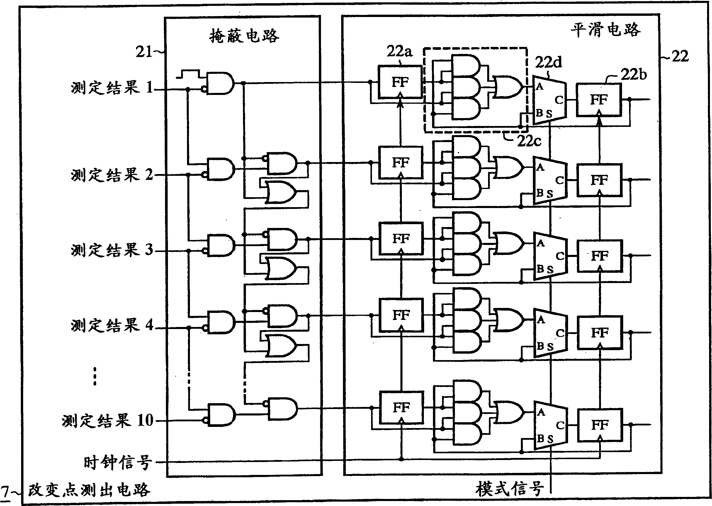
[0061] 6 is a measurement result storage circuit (measurement result storage unit), which is composed of a plurality of flip-flops (hereinafter referred to as FF) corresponding to each stage of the 1ns delay c...

Embodiment 2

[0103] Fig. 7 (a) is the explanatory diagram of the look-up table used as the correction signal generating part of Embodiment 2 of the present invention, and Fig. 7 (b) is the explanatory diagram of the theoretical delay corresponding to the number of elements obtained according to the look-up table; Figure 8 It is a characteristic diagram of the theoretical delay amount corresponding to the number of elements represented by a curve.

[0104]The look-up table shown in Fig. 5 (a) of the above-mentioned embodiment 1 provides that the delay about 1-level transistors is 0.2 ns, and they are divided into 22 groups for each 5-level group from 20 levels to 125 levels to generate 0 ns~ 3ns correction signal case. Figure 5(a) shows the design-determined number of stages and the actual delay obtained by each group. When sampling the output delay of each fixed number of delay stages, the part with a large number of delay stages is The increment of each stage is small, and the increment...

Embodiment 3

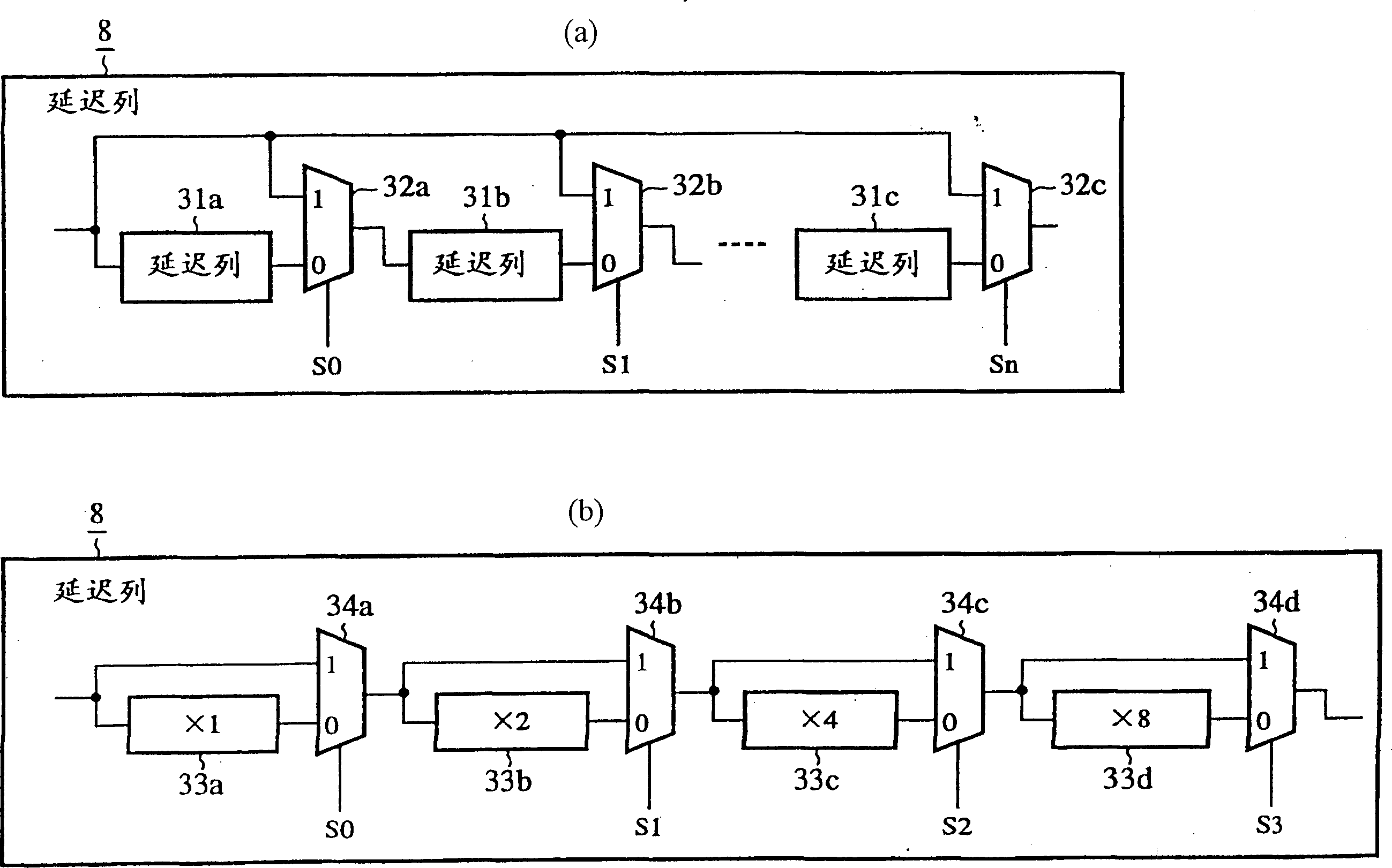
[0109] 9 is a circuit diagram showing an application example of a non-overlapping two-phase clock signal generating circuit of the delay adjustment circuit according to Embodiment 3 of the present invention, and 40 in the figure is a non-overlapping two-phase clock signal generating circuit (non-overlapping two-phase clock signal generating means) . 41a to 41j refer to inverters, 42a and 42b refer to "NAND" circuits, and 43a to 43h are selectors (delay components) which are set as feedback delay columns of the non-overlapping two-phase clock signal generating circuit 40 and whose number of connections can be adjusted freely. ). 44 is a decoder circuit that decodes the correction signal generated by the correction signal generation circuit 9 and is switched by the selectors 43a to 43h. Other structures are the same as those shown in Figure 1.

[0110] Next, the operation will be described.

[0111] In the third embodiment, an application example of the non-overlapping two-ph...


PUM


Abstract

A semiconductor device includes a delay amount measuring unit, multiple delay sections and a correction signal generating unit. The delay amount measuring unit for measures an actual delay amount corresponding to a specified delay amount by supplying a clock signal with a known period to multiple 1-ns-delay strings with a preassigned delay amount, and by detecting phase variations of the clock signal by the 1-ns-delay strings. The delay sections includes a delay string capable of freely adjusting a connection number of its delay elements. The correction signal generating unit generates a correction signal for enabling each of the delay sections to correct the connection number of the delay strings such that each delay section has a desired delay amount, in accordance with the actual delay amount corresponding to the specified delay amount and measured by the delay measuring unit.

Description

technical field [0001] The present invention relates to a semiconductor device capable of finely adjusting the amount of delay. technical background [0002] Figure 12 It is an explanatory diagram about the clock skew (SKEW) problem that occurred in the data transfer between two flip-flops in the past. Figure 13 (a) shows the timing diagram under normal conditions, Figure 13 (b) shows the time plot for the problematic case. [0003] Figure 12 In , the output of the flip-flop (hereinafter referred to as FF) has some delay before reaching the next FF. For example, as shown in the figure, a delay of 5 ns occurs at Q to Q1. In this example, when the clock signals of two FFs change at exactly the same timing, such as Figure 13 As shown in (a), the output of the second FF changes after one cycle. [0004] However, when there is a difference in the timing of changes in the two clock signals, such as Figure 13 (b) shows that when there is a 7ns delay at CK2, that is, whe...

Claims


Application Information

Patent Timeline
Patent Type & Authority Applications(China)
IPC IPC(8): G06F1/10H03K5/00H03K5/13H03K5/135H03K5/1532H03K5/1534
CPCH03K5/132H03K5/133H03K2005/00078H03K5/135G06F1/10G11C7/22
Inventor 矢泽弥亘中川伸一和田恭司
Owner MITSUBISHI ELECTRIC CORP
Why Eureka
Try Eureka