Plastic package base, air cavity type package and their manufacturing methods

A technology of plastic packaging and packaging substrates, which is applied in the direction of electrical components, electric solid devices, circuits, etc., can solve the problems of weak adhesion strength, increase in the number of molds, and air cavity plastic packaging can not meet the needs of more miniaturized packaging, so as to achieve simplification Craft, the effect of reducing the likelihood

Inactive Publication Date: 2003-10-15
SAHAVIRIYA STEEL INDUSTRIES
View PDF0 Cites 34 Cited by
  • Summary
  • Abstract
  • Description
  • Claims
  • Application Information

AI Technical Summary

Problems solved by technology

However, since each wall of the air cavity becomes thick after two molding processes for forming the first and second plastic bodies 44b and 44a are performed, the air cavity type plastic package cannot meet the demand for miniaturization of the package.
In addition, existing air cavity type plastic packages have other problems such as weak adhesion strength at the interface between the first plastic body 44b and the second plastic body 44a, increased number of molds, and expensive development costs.

Method used


Image

  • Plastic package base, air cavity type package and their manufacturing methods
  • Plastic package base, air cavity type package and their manufacturing methods
  • Plastic package base, air cavity type package and their manufacturing methods

Examples


no. 1 example

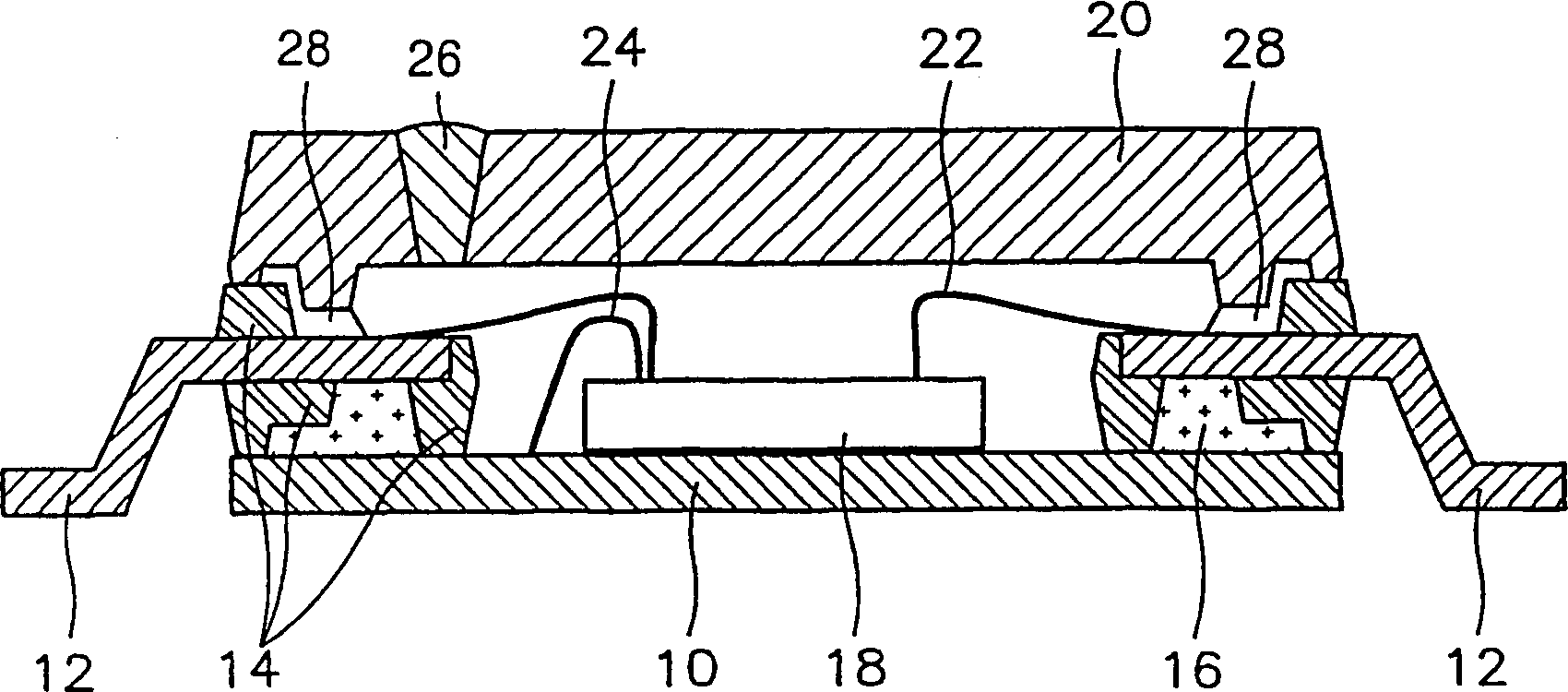
[0057] image 3 A cross-sectional view of an air cavity type plastic package according to a first embodiment of the present invention is shown. refer to image 3 , the first lead frame including the first leads 110a and the first pads 120 as internal terminals and the second lead frame including the second leads 210 and the second pads 220 as external terminals are bonded together with conductive solder. The chip 520 is bonded to the first pad 120 on the first lead frame with an adhesive (not shown), and is wire bonded to the first lead 110 a of the first lead frame with a bonding wire 503 .

[0058] The first and second lead frames are molded into a combined body with epoxy molding compound (EMC) plastic body 320 . Top surfaces of the first lead 110 a and the first pad 120 and bottom surfaces of the second lead 210 and the second pad 220 are exposed. The top surface of the plastic body 320 is flush with the top surfaces of the first lead 110 a and the first pad 120 .

[0...

no. 2 example

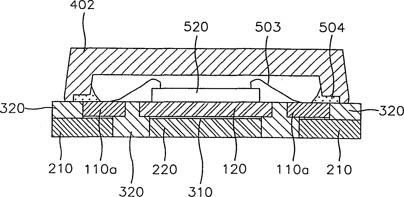
[0092] Figures 5 to 7 A sectional view showing a modification of the air cavity type plastic package according to the second embodiment of the present invention. The present invention is not limited to Figures 5 to 7 The illustrated air-cavity plastic package including various package substrates can be applied to other air-cavity plastic packages (not shown) having different package substrate structures.

[0093] refer to Figure 5 , the chip 520 is bonded to the package substrate 404 by means of an adhesive (not shown), and a bonding wire 503 is formed to electrically connect the chip 520 and the package substrate 404 . The plastic cover 410 is hermetically mounted on the package substrate with a sealant 450, thereby forming an air cavity. exist Figure 5 In , only the main components of the package substrate 404 are shown for convenience. However, in the package substrate 404 , a plurality of leads (not shown) may be formed to be electrically connected to external ter...


PUM


Abstract

A plastic package base, an air cavity type plastic package, and their manufacturing methods, which are capable of realizing the advantages of a ceramic package in that it has a compact size, makes less noise, and is highly thermally resistant, are provided. The plastic package base includes: a first lead frame including at least one first unit body comprising a first pad required for chip bonding and first leads acting as internal terminals, arranged around the first pad and spaced a predetermined distance away from the first pad; a second lead frame including at least one second unit body comprising a second pad and second leads acting as external terminals and bonded to the first lead frame so that the second pad and the second leads correspond to the first pad and first leads of the first lead frame; and a plastic body mold-shaped in spaces between the first and second lead frames so that the top surfaces of the first leads, the top surface of the first pad, the bottom surfaces of the second leads, and the bottom surface of the second pad are exposed on the surfaces of the plastic body and the top surface of the plastic body is not higher than the top surfaces of the first leads.

Description

technical field [0001] The present invention relates to a package accommodating a semiconductor chip therein, and more particularly to a plastic package substrate, an air cavity type package accommodating a semiconductor chip in an air cavity, and a manufacturing method thereof. Background technique [0002] Packages that house electrical or electronic devices, such as semiconductor devices, are divided into two different types, including ceramic packages and plastic packages. A ceramic package is an air cavity type package generally formed by filling the inside of the package with air in order to prevent the active surface of an electric or electronic device chip mounted therein from contacting the material of the package, while a plastic package is generally not an air cavity type. For devices with weak physical characteristics (due to contact with packaged materials, the expected functions and characteristics of such devices will be seriously degraded), electrically sensi...

Claims


Application Information

Patent Timeline
Patent Type & Authority Applications(China)
IPC IPC(8): H01L23/02H01L23/04H01L23/055H01L23/08H01L23/10H01L23/495H01L23/498H01L23/50
CPCH01L2924/01015H01L24/97H01L23/04H01L2924/01023H01L23/49537H01L2924/01082H01L23/10H01L2924/01004H01L2924/16152H01L2924/16315H01L24/48H01L2224/97H01L2224/32245H01L2924/01002H01L2224/48247H01L2224/49109H01L2924/01033H01L2924/01005H01L2924/01006H01L2924/01029H01L23/49861H01L2924/01078H01L2924/15151H01L2224/48257H01L2924/01075H01L2224/48091H01L23/055H01L2224/73265H01L2924/3025H01L2224/451H01L2924/00014H01L2924/181H01L24/45H01L2924/16151H01L2924/16195H01L24/49H01L2224/49171Y10T29/4913Y10T29/49144Y10T29/49121H01L2224/85H01L2924/00H01L2224/45099H01L2224/05599
Inventor 朴赞益
Owner SAHAVIRIYA STEEL INDUSTRIES
Why Eureka
Try Eureka